|
WLP200 same as SWTESD02-CSP ESD PROTECTED ANALOG RC FILTER SWTESD02-CSP manufactured by SEMICONWELL
FEATURES Six channels of EMI filtering All I/O pins are ESD protected Greater than 30dB attenuation over 800 to 2700 MHz band. +8kV ESD protection on each channel (IEC 61000-4-2 Level 4, contact discharge), +15kV ESD protection on each channel (HBM) Silicon substrate
Chip Scale Package features extremely low lead inductance for optimum filter and ESD performance
APPLICATIONS EMI filtering and ESD protection for audio ports Wireless Handsets Wireless Handsets Evaluation Devices
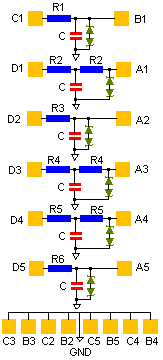
SHORT PRODUCT APPLICATION NOTE SWTESD-CSP consists of six RC filters with different filter characteristics in a wafer level package. All I/O pins are ESD protected for contact discharges up to 8KV per the IEC1000-4-2 level 4 specification. Two versions with different capacito values are available. This devices provides a minimum of -30dB over 800 to 2700 MHz band. The bumb size and pitch of these filters are selected such that the device can be placed directly on a FR4 printed circuit board using conventional assembly techniques. Ground-bounce and cross-talk are minimized by a die design that provides eight solder bump contacts to the common supply connection..
SEMICONDUCTOR-THIN FILM MANUFACTURING PROCESS DESCRIPTION
Integrated passive networks are manufactured using advanced thin film technologies including ultra -stable and self passivating Tantalum Nitride resistors, gold interconnect metallization and reliable MNOS capacitors to achieve excellent uniformity, performance and reliability. Thin film resistor technology is the preferred solution for all applications that require low noise, long term stability and excellent performance at very high frequencies. Semiconwell employs proprietary thin film technologies for deposition of a wide range of sheet resistance films from 1 W/sq to 10,000 W/sq. All Semiconwell's products are available in die form and as KGD, known good die and are ideal for high reliability hybrid and multi chip module applications. Besides thin film resistors, Semiconwell integrates capacitors, Schottky diodes, Zener diodes and transistors. Integrated passive and active networks are manufactured using Semiconwell's in house high reliability semiconductor manufacturing processes. All semiconductor devices employ precision doping via ion implantation, silicon nitride junction passivation, platinum silicided contacts and gold interconnect metallization for best performance and reliability. MNOS capacitors and Tantalum Nitride resistors are easily integrated with Schottky diodes to provide complete standard and custom RCD solutions. In die form, these products are ideal for hybrid and multi chip module applications. In packaged form, these products are the best solution where space and weight are a concern.
ABSOLUTE MAXIMUM RATINGS
Reverse voltage VR Continuous IF IFRM for tw<100ms Max Power dissipation 15V 100mA 200 mA (20%duty cycle) 100mW@70°C/Resistor Stresses beyond listed absolute maximum ratings may cause permanent damage to the device.
ELECTRICAL CHARACTERISTICS
Storage Temperature Range -65 to +150 °C
Operating Temperature Range -40 to +85 °C
DC Power per Resistor 100 mW
DC Package Power Rating 400 mW
Resistance Tolerance max. ±10 %
Capacitance Tolerance max.±20 %
Signal Voltage, Positive Clamp,I LOAD = 10mA
Signal Voltage,Negative Clamp
min.5 ; typ.7; max.15V
min.-5;typ.-10;max.-15V
In-system ESD Withstand Voltage,Notes 2,4 and 5
a) Human Body Model, MIL-STD-883,Method 3015 min.±15 kV
b) Contact Discharge per IEC 61000-4-2 Level 4 min.±8kV
Clamping Voltage during ESD Discharge MIL-STD-883 (Method 3015), 8kV;Notes 2,3,4 and 5
Positive Transients max. +30V
Negative Transients min. -30V
ELECTRICAL CHARACTERISTICS OF FILTERS Filter Filter Type Input Pin Output Pin R(W) C(pF) Fc(MHz)(Note6) Fc(MHz)(Note7)
Note 1: T A =25°C unless otherwise specified Note 2: ESD applied to input and output pins with respect to GND, one at a time. Note 3: Clamping voltage is measured at the opposite side of the EMI filter to the ESD pin.
Note 4: Unused pins are left open Note 5: The parameters are guaranteed by design and characterization Note 6.: Calculated with zero Source impedance and infinite Load impedance
Note 7: Calculated with 50 WSource impedance and 50W Load impedance.
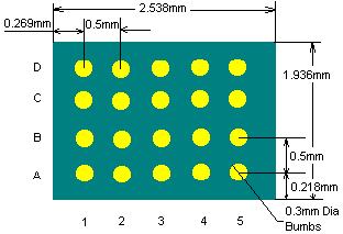
GENERAL DIE INFORMATION
SiO2 / Silicon 25±2 100 x 75±3 4x4 mils, 3mm thick, 99.99% electroplated gold with a TiW barrier Au/Si compatible with eutectic and conductive epoxy die attach.
All Semiconwell products are available in die form for chip and wire hybrid circuits and multi chip modules applications. Typical delivery for standard die products is 3-4 weeks ARO. For Chip Scale Packaged (CSP) devices consult factory for an update on availability of certain products.
The protection diodes use solid state silicon avalanche technology and are characterized by their high surge capability, low operating and clamping voltages, fast response time and low leakage current Ultra stable TaN with low TCR <75ppm/°C typical. For Rsq<10W/sq and Rsq>500W/sq, resistive material is proprietary. Power rating/resistor max 100mW for R<1KW and 25mW for R>1KW. Standard tolerance is ±5%. Silicon nitride dielectric, MNOS capacitors exhibit high stability, low temperature coefficients, low leakage <10nA and high BV>50V.
STANDARD PRODUCTS ORDERING INFORMATION SW PART# SWTEDS002-CSP
Delivery for packaged RCD standard products is 6-8 weeks ARO. Certain items may be available from stock. For standard products available from stock, there is a minimum line item order of $250.0. Inventory is periodically updated. For 2500pc or larger orders, all surface mount packaged devices are shipped in tape on reel (T/R). For smaller quantities, it may vary. Samples are available only for customers that have issued firm orders pending qualification of product in a particular application. On line Orders have to be verified, accepted and acknowledged by Semiconwell sales department in writing before, becoming non cancelable binding contracts.
Semiconwell guarantees continuous supply and availability of any of it's standard products provided minimum order quantities are met.
SEMICONWELL has made every effort to have this information as accurate as possible. However, no responsibility is assumed by SEMICONWELL for its use, nor for any infringements of rights of third parties which may result from its use. SEMICONWELL reserves the right to revise the content or modify its product line without prior notice. SEMICONWELL products are not authorized for and should not be used within support systems which are intended for surgical implants into the body, to support or sustain life, in aircraft, space equipment, submarine, or nuclear facility applications without the specific written consent.
|