|
CLAMP SCHOTTKY DIODE NETWORK 500mA, 16 CHANNELS SWDN5016-20
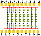
FEATURES APPLICATIONS SCHEMATIC
32 integrated diodes in a single package offers 16 channels, dual rail clamping action PCI v2.1 Bus Termination for Intel-based Pentium® and Pentium Pro systems
Provides proper bus termination independent of external line or card loading conditions Local high speed bus termination for most RISC and embedded microprocessor applications
Schottky diode technology; excellent forward voltage and reverse recovery characteristics Saves board space and eases layout in space critical bus termination applications versus discrete approaches Local high speed bus termination for most RISC and embedded microprocessor applications
High speed memory DRAM, SDRAM, EPROM memory bus termination
Termination of high speed CLOCK lines of multiple clocked devices.
SHORT PRODUCT APPLICATION NOTE
Integrated clamp Schottky diode network is a low power and low noise solution for reducing reflections on high speed data lines. Reflection on high speed data lines leads to undershoot and overshoot disturbances which may result in improper system operation. Resistor terminations used in parallel or in series with the outputs, when used to terminate high speed data lines, can increase power consumption, degrade the high level output and lower noise immunity or increase propagation delays. Schottky diode termination is the best overall solution for applications in which power consumption and noise immunity are critical considerations. Clamp Schottky diode networks provide optimized lead inductance and parasitic capacitive effects (see added ground pins), improved forward voltage and crosstalk attributes, and best termination performance characteristics at high data transmission rates.
SEMICONDUCTOR-THIN FILM MANUFACTURING PROCESS DESCRIPTION
Integrated passive networks are manufactured using advanced thin film technologies including ultra -stable and self passivating Tantalum Nitride resistors, gold interconnect metallization and reliable MNOS capacitors to achieve excellent uniformity, performance and reliability. Thin film resistor technology is the preferred solution for all applications that require low noise, long term stability and excellent performance at very high frequencies. Semiconwell employs proprietary thin film technologies for deposition of a wide range of sheet resistance films from 1W/sq to 10,000 W/sq. All Semiconwell's products are available in die form and as KGD, known good die and are ideal for high reliability hybrid and multi chip module applications. Besides thin film resistors, Semiconwell integrates capacitors, Schottky diodes, Zener diodes and transistors. Integrated passive and active networks are manufactured using Semiconwell's in house high reliability semiconductor manufacturing processes. All semiconductor devices employ precision doping via ion implantation, silicon nitride junction passivation, platinum silicided contacts and gold interconnect metallization for best performance and reliability. MNOS capacitors and Tantalum Nitride resistors are easily integrated with Schottky diodes to provide complete standard and custom RCD solutions. In die form, these products are ideal for hybrid and multi chip module applications. In packaged form, these products are the best solution where space and weight are a concern.
ABSOLUTE MAXIMUM RATINGS
Reverse voltage VR Continuous IF IFRM for tw<100ms Max Power dissipation
7V 500mA 200 mA (20%duty cycle) 100mW@70°C/channel
Stresses beyond listed absolute maximum ratings may cause permanent damage to the device.
ELECTRICAL CHARACTERISTICS
PARAMETER VALUE UNITS
Supply Voltage (VDD) -0.3...+7 V
Voltage at any Channel Input (Vsignal) -0.3...(VDD+0.3) V
Channel Clamp Current ( Iclamp) ±500 mA
Power Dissipation (IF< 10mA/Channel; TA=25°C) (Pd) 1 W
Operating Temperature (TOP) 0 to 70 °C
Storage Temperature (Tstg) -65 to +150 °C
Diode Forward Voltage to VDD (IF=500mA) typ. 0.95 V
Diode Forward Voltage from GND (IF = 600mA) typ. 1.5 V
Channel Leakage(0500W/sq, resistive material is proprietary. Power rating/resistor max 100mW for R<1KW and 25mW for R>1KW. Standard tolerance is ±5%. Silicon nitride dielectric, MNOS capacitors exhibit high stability, low temperature coefficients, low leakage <10nA and high BV>50V.
DIE LAYOUT PACKAGE PIN OUT
Layout pending
Vin=2,3,4,5,6,7,8,9,12,13,14,15,16,17,18,19
Vss=die backside
Vss=1,11
Vdd=10,20
STANDARD PRODUCTS ORDERING INFORMATION
SW PART # QUANTITY QSOP-16 U/P($) PDIP-16 U/P($) BARE DIE U/P($)
SWDN5016 1000pc -20QS $0.79 -20DP $0.87 -20BD $1.29
SWDN5016 2000pc -20QS $0.71 -20DP $0.79 -20BD $1.21
SWDN5016 5000pc -20QS $0.62 -20DP $0.70 -20BD $1.12
SWDN5016 10,000pc -20QS $0.55 -20DP $0.63 -20BD $1.05
For special packaging or custom configurations, contact sw_sales@semiconwell.com
Delivery for packaged RCD standard products is 6-8 weeks ARO. Certain items may be available from stock. For standard products available from stock, there is a minimum line item order of $250.0. Inventory is periodically updated. For 2500pc or larger orders, all surface mount packaged devices are shipped in tape on reel (T/R). For smaller quantities, it may vary. Samples are available only for customers that have issued firm orders pending qualification of product in a particular application. On line Orders have to be verified, accepted and acknowledged by Semiconwell sales department in writing before, becoming non cancelable binding contracts.
Semiconwell guarantees continuous supply and availability of any of it's standard products provided minimum order quantities are met.
SEMICONWELL has made every effort to have this information as accurate as possible. However, no responsibility is assumed by SEMICONWELL for its use, nor for any infringements of rights of third parties which may result from its use. SEMICONWELL reserves the right to revise the content or modify its product line without prior notice. SEMICONWELL products are not authorized for and should not be used within support systems which are intended for surgical implants into the body, to support or sustain life, in aircraft, space equipment, submarine, or nuclear facility applications without the specific written consent.
|