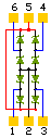
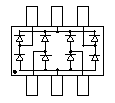
SWDNZ1004, QSBT40 EQUIVALENT, 4 channels, 200mA, esd protected Schottky diode array available in surface mount package and as known good die KGD is a low power and low noise solution for reducing reflections on high speed data lines. Reflection on high speed data lines leads to undershoot and overshoot disturbances which may result in improper system operation. Resistor terminations used in parallel or in series with the outputs, when used to terminate high speed data lines, can increase power consumption, degrade the high level output and lower noise immunity or increase propagation delays. Schottky diode termination is the best overall solution for applications in which power consumption and noise immunity are critical considerations. Clamp Schottky diode networks provide optimized lead inductance and parasitic capacitive effects (see added ground pins), improved forward voltage and crosstalk attributes, and best termination performance characteristics at high data transmission rates.Schottky diode networks are manufactured using Semiconwell's in house high reliability semiconductor manufacturing processes. All semiconductor devices employ precision doping via ion implantation, silicon nitride junction passivation, platinum silicided contacts and gold interconnect metallization for best performance and reliability. MNOS capacitors and Tantalum Nitride resistors are easily integrated with Schottky diodes to provide complete standard and custom RCD solutions. In die form, these products are ideal for hybrid and multi chip module applications. In packaged form, these products are the best solution where space and weight are a concern. . For special packaging or custom configurations, contact sw_sales@semiconwell.com. 8 integrated diodes in a single package offers 4 channels, dual rail clamping action.Provides proper bus termination independent of external line or card loading conditions. Schottky diode technology; excellent forward voltage and reverse recovery characteristics. Saves board space and eases layout in space critical bus termination applications versus discrete approaches. PCI v2.1 Bus Termination for Intel-based Pentium® and Pentium Pro systems. Local high speed bus termination for all popular RISC and embedded microprocessor applications. High speed memory DRAM, SDRAM, EPROM memory bus termination. Termination of high speed CLOCK lines of multiple clocked devices.


SEMICONWELL
Integrated Passive Networks
  ESD PROTECTED SCHOTTKY DIODE ARRAY
200mA, 4 CHANNELS

SWDNZ1004


FEATURES
APPLICATIONS
SCHEMATIC
Low Forward Voltage Drop
Fast Switching
Very High Density
Ultra-Small Surface Mount Package and Bare Die
PN Junction Guard Ring for Transient and ESD Protection
Provide transient protection for high-speed data lines in accordance with:
IEC61000-4-2 (ESD)15kV (Air),8kV (Contact)
IEC61000-4-4 (EFT)80A (tp =5/50 ns)
IEC61000-4-5 (Lightning) Class 3
PCI v2.1 Bus Termination for Intel-based Pentium® and Pentium Pro systems
Local high speed bus termination for most RISC and embedded microprocessor applications
High speed memory DRAM, SDRAM, EPROM memory bus termination
Termination of high speed CLOCK lines of multiple clocked devices.
schematic

SHORT PRODUCT APPLICATION NOTE
ESD protected Schottky diode network is a low power and low noise solution for reducing reflections on high speed data lines. Reflection on high speed data lines leads to undershoot and overshoot disturbances which may result in improper system operation. Resistor terminations used in parallel or in series with the outputs, when used to terminate high speed data lines, can increase power consumption, degrade the high level output and lower noise immunity or increase propagation delays. Schottky diode termination is the best overall solution for applications in which power consumption and noise immunity are critical considerations. Clamp Schottky diode networks provide optimized lead inductance and parasitic capacitive effects (see added ground pins), improved forward voltage and crosstalk attributes, and best termination performance characteristics at high data transmission rates.

SEMICONDUCTOR-THIN FILM MANUFACTURING PROCESS DESCRIPTION
Schottky diode networks are manufactured using Semiconwell's in house high reliability semiconductor manufacturing processes. All semiconductor devices employ precision doping via ion implantation, silicon nitride junction passivation, platinum silicided contacts and gold interconnect metallization for best performance and reliability. MNOS capacitors and Tantalum Nitride resistors are easily integrated with Schottky diodes to provide complete standard and custom RCD solutions. In die form, these products are ideal for hybrid and multi chip module applications. In packaged form, these products are the best solution where space and weight are a concern.

ABSOLUTE MAXIMUM RATINGS
Reverse voltage VR Continuous IF IFRM for tw<1000ms Max Power dissipation
30V 200mA 600 mA (20%duty cycle) 200mW@70°C/channel

Stresses beyond listed absolute maximum ratings may cause permanent damage to the device.

ELECTRICAL CHARACTERISTICS
PARAMETER VALUE UNITS
Supply Voltage (VDD) -0.3...+30 V
Voltage at any Channel Input (Vsignal) -0.3...(VDD+0.3) V
Channel Clamp Current ( Iclamp) ±200 mA
Power Dissipation (IF< 10mA/Channel; TA=25°C) (Pd) 1 W
Operating Temperature (TOP) 0 to 70 °C
Storage Temperature (Tstg) -65 to +150 °C
Diode Forward Voltage @ IF=10mA max. 0.45 V
Diode Forward Voltage @ IF=30mA max. 0.55 V
Channel Leakage(0<Vin<VDD) typ. 1 max. 10 mA
Input capacitance @1MHz, VR=0V <10 pF
Reverse recovery time @IF=10mA 5 ns

GENERAL DIE INFORMATION
Substrate Thickness (mils) Die size (mils) Bonding pads Backside metal
Silicon 10±2 xx x yy ±3 4x4 mils, 3mm thick, 99.99% electroplated gold with a TiW barrier Au/Si compatible with eutectic and conductive epoxy die attach.
All Semiconwell products are available in die form for chip and wire hybrid circuits and multi chip modules applications. Typical delivery for die products is 6 weeks ARO. For Chip Scale Packaged (CSP) devices consult factory for an update on availability of certain products.

SCHOTTKY DIODES RESISTORS CAPACITORS
Schottky diodes offer basic ESD protection, with low forward voltage, low leakage and low power dissipation in OFF state. Schottky Diodes exhibit low junction capacitance CTand low on resistance RDON. Ultra stable TaN with low TCR <75ppm/°C typical. For Rsq<10W/sq and Rsq>500W/sq, resistive material is proprietary. Power rating/resistor max 100mW for R<1KW and 25mW for R>1KW. Standard tolerance is ±5%. Silicon nitride dielectric, MNOS capacitors exhibit high stability, low temperature coefficients, low leakage <10nA and high BV>50V.

DIE LAYOUT PACKAGE PIN OUT
layout schematic
Vin=1,3,4,6
Vss=die backside
Vss=2
Vdd=5

STANDARD PRODUCTS ORDERING INFORMATION

SW PART # QUANTITY SOT26 U/P($) SOT326 U/P($) SC70-6 U/P($) BARE DIE U/P($)
SWDNZ1004 5000pc -SOT26 - -SOT326 - -SC706 - -6BD -
SWDNZ1004 10,000pc -SOT26 - -SOT326 - -SC706 - -6BD -
For products sold as bare tested die or known good die KGD, minimum order is 5000pc. Dice are 100% functional tested, visual inspected and shipped in antistatic waffle packs. For special die level KGD requirements, different packaging or custom configurations, contact sw_sales@semiconwell.com

  Semiconwell P/N Quantity E-mail    
Receive Instant Quote
 

Delivery for packaged RCD standard products is 6-8 weeks ARO. Certain items may be available from stock. For standard products available from stock, there is a minimum line item order of $250.0. Inventory is periodically updated. For 2500pc or larger orders, all surface mount packaged devices are shipped in tape on reel (T/R). For smaller quantities, it may vary. Samples are available only for customers that have issued firm orders pending qualification of product in a particular application. On line Orders have to be verified, accepted and acknowledged by Semiconwell sales department in writing before, becoming non cancelable binding contracts.

Semiconwell guarantees continuous supply and availability of any of it's standard products provided minimum order quantities are met.

SEMICONWELL has made every effort to have this information as accurate as possible. However, no responsibility is assumed by SEMICONWELL for its use, nor for any infringements of rights of third parties which may result from its use. SEMICONWELL reserves the right to revise the content or modify its product line without prior notice. SEMICONWELL products are not authorized for and should not be used within support systems which are intended for surgical implants into the body, to support or sustain life, in aircraft, space equipment, submarine, or nuclear facility applications without the specific written consent.

Home Product Tree Tech. Support Print PDF Packages Request Quote Inventory Place Order Contact sales