| FEATURES |
| APPLICATIONS |
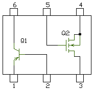
| SCHEMATIC |
| Combines MMBT4403 type transistor with 2N7002 type MOSFET |
| Small Surface Mount Package |
| NPN/P-Channel Complement Available:CTA2N1P |
| Case:SOT-326 |
| SW CTA2P1N MMBT4403 PNP TRANSISTOR AND 2N7002 N-CHANNEL MOSFET COMPLEX ARRAY FEATURES Combines MMBT4403 type transistor with 2N7002 type MOSFET Small Surface Mount Package NPN/P-Channel Complement Available:CTA2N1P Case:SOT-326 SEMICONDUCTOR-THIN FILM MANUFACTURING PROCESS DESCRIPTION Integrated passive networks are manufactured using advanced thin film technologies including ultra -stable and self passivating Tantalum Nitride resistors, gold interconnect metallization and reliable MNOS capacitors to achieve excellent uniformity, performance and reliability. Thin film resistor technology is the preferred solution for all applications that require low noise, long term stability and excellent performance at very high frequencies. Semiconwell employs proprietary thin film technologies for deposition of a wide range of sheet resistance films from 1W/sq to 10,000 W/sq. All Semiconwell's products are available in die form and as KGD, known good die and are ideal for high reliability hybrid and multi chip module applications. Besides thin film resistors, Semiconwell integrates capacitors, Schottky diodes, Zener diodes and transistors. Integrated passive and active networks are manufactured using Semiconwell's in house high reliability semiconductor manufacturing processes. All semiconductor devices employ precision doping via ion implantation, silicon nitride junction passivation, platinum silicided contacts and gold interconnect metallization for best performance and reliability. MNOS capacitors and Tantalum Nitride resistors are easily integrated with Schottky diodes to provide complete standard and custom RCD solutions. In die form, these products are ideal for hybrid and multi chip module applications. In packaged form, these products are the best solution where space and weight are a concern. ABSOLUTE MAXIMUM RATINGSTA = 25 °C unless otherwise specified PARAMETER VALUE UNITS Power Dissipation (Note 1) 150 mW TstgStorageTemperature Range -55 to +150 °C TambOperating Ambient Temperature Range -55 to +150 °C Tjjunction temperature max. +150 °C THERMAL CHARACTERISTICS PER DEVICE Rth j-athermal resistance from junction to ambient. 833 °C/W Maximum Ratings,Q1,MMBT4403 PNP Transistor Element @TA =25°C unless otherwise specified Collector-Base Voltage -40 V Collector-Emitter Voltage -40 V Emitter-Base Voltage -5 V Collector Current -Continuous -600 mA Maximum Ratings,Q2,2N7002NP-Channel MOSFET Element @TA =25°C unless otherwise specified Drain-Source Voltage -50 V Drain-Gate Voltage RGS <= 1.0MW -50 V Gate-Source Voltage Continuous Pulsed ±20 ±40 V Drain Current Continuous, note 1,Continuous Continuous @100 °C Pulsed 115 73 800 mA Note 1:Device mounted on FR-4 PCB . Stresses beyond listed absolute maximum ratings may cause permanent damage to the device. ELECTRICAL CHARACTERISTICS,TVS Element, Tamb =25°C unless specified. PARAMETER VALUE UNITS Electrical Characteristics,Q1,MMBT4403 PNP Transistor Element Collector-Base Breakdown Voltage,IC =-100mA,IE =0 min.-40 V Collector-Emitter Breakdown Voltage,IC =-1.0mA,IB =0 min.-40 V Emitter-Base Breakdown Voltage,IE =-100 mA, IC =0 min.-5 V Collector Cutoff Current,VCE =-35V,VEB(OFF)=-0.4V max.-100 nA Base Cutoff Current, VCE =-35V,VEB(OFF)=-0.4V max.-100 nA DC Current Gain IC =-100 µA,VCE =-1.0V IC =-1.0mA,VCE =-1.0V IC =-10mA,VCE =-1.0V IC =-150mA,VCE =-2.0V IC =-500mA,VCE =-2.0V min.30 min.60 min.100 min.100 max.300 min.20 Collector-Emitter Saturation Voltage, IC =-150mA,IB =-15mA IC =-500mA,IB =-50mA max.-0.4 max.-0.75 V V Base-Emitter Saturation Voltage IC =-150mA,IB =-15mA IC =-500mA,IB =-50mA min.-0.75 max.-0.95 max.-1.3 V V Output Capacitance,Ccb, VCB =-10.0V,f =1.0MHz,IE =0 max.8.5 pF Input Capacitance,Ceb,VEB =-0.5V,f =1.0MHz,IC =0 max.30 pF Input Impedance hie, VCE =-10V,IC =-1.0mA,f =1.0kHz min.1.5 max. 15 kW Voltage Feedback Ratio hre,VCE =-10V,IC =-1.0mA,f =1.0kHz min.0.1 max. 8 x10⁻⁴ Small Signal Current Gain hfe,VCE =-10V,IC =-1.0mA,f =1.0kHz min.60 max.500 Output Admittance hoe,VCE =-10V,IC =-1.0mA,f =1.0kHz min. 1 max.100 mS Current Gain-Bandwidth Product fT,VCE =-10V,IC =-20mA,f =100MHz min.200 MHz Delay Time td,VCC =-30V,IC =-150mA,VBE(off)=-2.0V,IB1 =-15mA max.15 ns Rise Time tr,VCC =-30V,IC =-150mA,VBE(off)=-2.0V,IB1 =-15mA max.20 ns Storage Time ts,VCC =-30V,IC =-150mA,IB1 =IB2 =-15mA max.225 sn Fall Time tf,VCC =-30V,IC =-150mA,IB1 =IB2 =-15mA max.30 ns Electrical Characteristics,Q2, 2N7002N-Channel MOSFET Element Drain-Source Breakdown Voltage BVDSS,VGS =0V,ID =250 µA,note 2 min.50 V Zero Gate Voltage Drain Current, note 2 VDS =60V,VGS =0V,TJ =25°C VDS =60V,VGS =0V,TJ =125 °C max.1 max.500 mA mA Gate-Body Leakage IGSS,VGS =±20V, VDS =0V,note 2 max.±10 nA Gate Threshold Voltage VGS(th),VDS =VGS,ID =-0.25mA, note 2 min.1 max.2 V Static Drain-Source On-Resistance RDS(ON),,note 2 Tj =25 °C,VGS =5V,ID =0.05A, Tj =125 °C,VGS =10V,ID =0.5A typ.3.2 max.7,5 typ.4,4 max.13.5 W On-State Drain Current ID(ON),VGS =10V,VDS =7.5V min. 0.5 typ. 1 A Forward Transconductance gFS,VDS =10V,ID =0.2A, note 3 min.80 mS Input Capacitance Ciss,VDS =25V,VGS =0V,f=1MKz typ.22 max.50 pF Output Capacitance Coss,VDS =25V,VGS =0V,f=1MKz typ.11 max.25 pF Reverse Transfer Capacitance Crss,VDS =25V,VGS =0V,f=1MKz typ.2 max.5 pF Turn-On Delay Time tD(ON),VDD =30V,ID =0.2A,RL =150 W, VGS =10V,RGEN =25 W typ.7 max.20 ns Turn-Off Delay Time tD(OFF),VDD =30V,ID =0.2A,RL =150 W, VGS =10V,RGEN =25 W typ.11 max.20 ns Note 2:Short duration pulse test used to minimize self-heating effect. GENERAL DIE INFORMATION Substrate Thickness (mils) Die size (mils) Bonding pads Backside metal Silicon ±0.5 ±1 4x4 mils, 3mm thick, 99.99% electroplated gold with a TiW barrier Au/Si compatible with eutectic and conductive epoxy die attach. All Semiconwell products are available in die form for chip and wire hybrid circuits and multi chip modules applications. Typical delivery for standard die products is 3-4 weeks ARO. For Chip Scale Packaged (CSP) devices consult factory for an update on availability of certain products. SEMICONDUCTORS RESISTORS CAPACITORS All semiconductor devices employ precision doping via ion implantation, silicon nitride junction passivation, platinum silicided contacts and gold interconnect metallization for best performance and reliability. Ultra stable TaN with low TCR < 75ppm/°C typical. For Rsq< 10W/sq and Rsq>500W/sq, resistive material is proprietary. Power rating/resistor max 100mW for R<1KW and 25mW for R>1KW. Standard tolerance is ±5%. Silicon nitride dielectric, MNOS capacitors exhibit high stability, low temperature coefficients, low leakage 10nA and high BV 50V. DIE LAYOUT PACKAGE PIN OUT STANDARD PRODUCTS ORDERING INFORMATION SOT326 SOT26 BARE DIE SW CTA2P1N-SOT326 SW CTA2P1NSOT26 SW CTA2P1N-BD SW PART # QUANTITY SOT-326 U/P($) SOT-26 U/P($) BARE DIE U/P($) SW CTA2P1N 5,000pc -SOT326 -SOT26 -BD SW CTA2P1N 10,000pc -SOT326 -SOT26 -BD For products sold as bare tested die or known good die KGD, minimum order is 5000pc. Dice are 100% functional tested, visual inspected and shipped in antistatic waffle packs. For special die level KGD requirements, different packaging or custom configurations, contact sw_sales@semiconwell.com Semiconwell P/N Quantity E-mail Receive Instant Quote -SOT326 -SOT26 -BD Delivery for packaged RCD standard products is 6-8 weeks ARO. Certain items may be available from stock. For standard products available from stock, there is a minimum line item order of $250.0. Inventory is periodically updated. For 2500pc or larger orders, all surface mount packaged devices are shipped in tape on reel (T/R). For smaller quantities, it may vary. Samples are available only for customers that have issued firm orders pending qualification of product in a particular application. On line Orders have to be verified, accepted and acknowledged by Semiconwell sales department in writing before, becoming non cancelable binding contracts. Semiconwell guarantees continuous supply and availability of any of it's standard products provided minimum order quantities are met. SEMICONWELL has made every effort to have this information as accurate as possible. However, no responsibility is assumed by SEMICONWELL for its use, nor for any infringements of rights of third parties which may result from its use. SEMICONWELL reserves the right to revise the content or modify its product line without prior notice. SEMICONWELL products are not authorized for and should not be used within support systems which are intended for surgical implants into the body, to support or sustain life, in aircraft, space equipment, submarine, or nuclear facility applications without the specific written consent. |
| SEMICONWELL
Integrated Passive Networks |
MMBT4403
PNP TRANSISTOR AND 2N7002 N-CHANNEL MOSFET COMPLEX ARRAY SW CTA2P1N |
|
|
|
|
||||||||||||
|
|
|
| SHORT PRODUCT APPLICATION NOTE |
| Integrated clamp Schottky diode network is a low power and low noise solution for reducing reflections on high speed data lines. Reflection on high speed data lines leads to undershoot and overshoot disturbances which may result in improper system operation. Resistor terminations used in parallel or in series with the outputs, when used to terminate high speed data lines, can increase power consumption, degrade the high level output and lower noise immunity or increase propagation delays. Schottky diode termination is the best overall solution for applications in which power consumption and noise immunity are critical considerations. Clamp Schottky diode networks provide optimized lead inductance and parasitic capacitive effects (see added ground pins), improved forward voltage and crosstalk attributes, and best termination performance characteristics at high data transmission rates. |
| SEMICONDUCTOR-THIN FILM MANUFACTURING PROCESS DESCRIPTION |
| Integrated passive networks are manufactured using advanced thin film technologies including ultra -stable and self passivating Tantalum Nitride resistors, gold interconnect metallization and reliable MNOS capacitors to achieve excellent uniformity, performance and reliability. Thin film resistor technology is the preferred solution for all applications that require low noise, long term stability and excellent performance at very high frequencies. Semiconwell employs proprietary thin film technologies for deposition of a wide range of sheet resistance films from 1W/sq to 10,000 W/sq. All Semiconwell's products are available in die form and as KGD, known good die and are ideal for high reliability hybrid and multi chip module applications. Besides thin film resistors, Semiconwell integrates capacitors, Schottky diodes, Zener diodes and transistors. Integrated passive and active networks are manufactured using Semiconwell's in house high reliability semiconductor manufacturing processes. All semiconductor devices employ precision doping via ion implantation, silicon nitride junction passivation, platinum silicided contacts and gold interconnect metallization for best performance and reliability. MNOS capacitors and Tantalum Nitride resistors are easily integrated with Schottky diodes to provide complete standard and custom RCD solutions. In die form, these products are ideal for hybrid and multi chip module applications. In packaged form, these products are the best solution where space and weight are a concern. |
| ABSOLUTE MAXIMUM RATINGSTA = 25 °C unless otherwise specified | ||
| PARAMETER | VALUE | UNITS |
Power Dissipation (Note 1) |
150 | mW |
TstgStorageTemperature Range |
|
|
TambOperating Ambient Temperature Range |
|
|
Tjjunction temperature |
|
|
THERMAL CHARACTERISTICS PER DEVICE |
||
Rth j-athermal resistance from junction to ambient. |
833
|
|
Maximum Ratings,Q1,MMBT4403 PNP Transistor Element @TA =25°C unless otherwise specified |
||
Collector-Base Voltage |
-40 |
V |
Collector-Emitter Voltage |
-40 |
V |
Emitter-Base Voltage |
-5 |
V |
Collector Current -Continuous |
-600 |
mA |
|
Maximum Ratings,Q2,2N7002NP-Channel MOSFET Element @TA =25°C unless otherwise specified |
||
Drain-Source Voltage |
-50 |
V |
Drain-Gate Voltage RGS </= 1.0MW |
-50 |
V |
Gate-Source Voltage Continuous Pulsed |
±20 ±40 |
V |
Drain Current Continuous, note 1,Continuous Continuous @100 °C Pulsed |
115 73 800 |
mA |
Note 1:Device mounted on FR-4 PCB . |
||
| Stresses beyond listed absolute maximum ratings may cause permanent damage to the device. |
| ELECTRICAL CHARACTERISTICS,TVS Element, Tamb =25°C unless specified. | ||
| PARAMETER | VALUE | UNITS |
| Electrical Characteristics,Q1,MMBT4403 PNP Transistor Element | ||
| Collector-Base Breakdown Voltage,IC =-100mA,IE =0 | min.-40 |
V |
| Collector-Emitter Breakdown Voltage,IC =-1.0mA,IB =0 | min.-40 |
V |
| Emitter-Base Breakdown Voltage,IE =-100 mA, IC =0 | min.-5 |
V |
| Collector Cutoff Current,VCE =-35V,VEB(OFF)=-0.4V | max.-100 |
nA |
| Base Cutoff Current, VCE =-35V,VEB(OFF)=-0.4V | max.-100 |
nA |
| DC Current Gain IC =-100 µA,VCE =-1.0V IC =-1.0mA,VCE =-1.0V IC =-10mA,VCE =-1.0V IC =-150mA,VCE =-2.0V IC =-500mA,VCE =-2.0V |
min.30 min.60 min.100 min.100 max.300 min.20 |
|
| Collector-Emitter Saturation Voltage, IC =-150mA,IB =-15mA IC =-500mA,IB =-50mA |
max.-0.4 max.-0.75 |
V V |
| Base-Emitter Saturation Voltage IC =-150mA,IB =-15mA IC =-500mA,IB =-50mA |
min.-0.75 max.-0.95 max.-1.3 |
V V |
| Output Capacitance,Ccb, VCB =-10.0V,f =1.0MHz,IE =0 | max.8.5 |
pF |
| Input Capacitance,Ceb,VEB =-0.5V,f =1.0MHz,IC =0 | max.30 |
pF |
| Input Impedance hie, VCE =-10V,IC =-1.0mA,f =1.0kHz | min.1.5 max. 15 |
kW |
| Voltage Feedback Ratio hre,VCE =-10V,IC =-1.0mA,f =1.0kHz | min.0.1 max. 8 |
x10-4 |
| Small Signal Current Gain hfe,VCE =-10V,IC =-1.0mA,f =1.0kHz | min.60 max.500 |
|
| Output Admittance hoe,VCE =-10V,IC =-1.0mA,f =1.0kHz | min. 1 max.100 |
mS |
| Current Gain-Bandwidth Product fT,VCE =-10V,IC =-20mA,f =100MHz | min.200 |
MHz |
| Delay Time td,VCC =-30V,IC =-150mA,VBE(off)=-2.0V,IB1 =-15mA | max.15 |
ns |
| Rise Time tr,VCC =-30V,IC =-150mA,VBE(off)=-2.0V,IB1 =-15mA | max.20 |
ns |
| Storage Time ts,VCC =-30V,IC =-150mA,IB1 =IB2 =-15mA | max.225 |
sn |
| Fall Time tf,VCC =-30V,IC =-150mA,IB1 =IB2 =-15mA | max.30 |
ns |
| Electrical Characteristics,Q2, 2N7002N-Channel MOSFET Element | ||
| Drain-Source Breakdown Voltage BVDSS,VGS =0V,ID =250 µA,note 2 | min.50 |
V |
| Zero Gate Voltage Drain Current, note 2 VDS =60V,VGS =0V,TJ =25°C VDS =60V,VGS =0V,TJ =125 °C |
max.1 max.500 |
mA mA |
| Gate-Body Leakage IGSS,VGS =±20V, VDS =0V,note 2 | max.±10 |
nA |
| Gate Threshold Voltage VGS(th),VDS =VGS,ID =-0.25mA, note 2 | min.1 max.2 |
V |
| Static Drain-Source On-Resistance RDS(ON),,note 2 Tj =25 °C,VGS =5V,ID =0.05A, Tj =125 °C,VGS =10V,ID =0.5A |
typ.3.2 max.7,5 typ.4,4 max.13.5 |
W |
| On-State Drain Current ID(ON),VGS =10V,VDS =7.5V | min. 0.5 typ. 1 |
A |
| Forward Transconductance gFS,VDS =10V,ID =0.2A, note 3 | min.80 |
mS |
| Input Capacitance Ciss,VDS =25V,VGS =0V,f=1MKz | typ.22 max.50 |
pF |
| Output Capacitance Coss,VDS =25V,VGS =0V,f=1MKz | typ.11 max.25 |
pF |
| Reverse Transfer Capacitance Crss,VDS =25V,VGS =0V,f=1MKz | typ.2 max.5 |
pF |
| Turn-On Delay Time tD(ON),VDD =30V,ID =0.2A,RL =150 W, VGS =10V,RGEN =25 W | typ.7 max.20 |
ns |
| Turn-Off Delay Time tD(OFF),VDD =30V,ID =0.2A,RL =150 W, VGS =10V,RGEN =25 W | typ.11 max.20 |
ns |
|
Note 2:Short duration pulse test used to minimize self-heating effect. |
||
| GENERAL DIE INFORMATION | ||||
| Substrate | Thickness (mils) | Die size (mils) | Bonding pads | Backside metal |
| Silicon | ±0.5 | ±1 | 4x4 mils, 3mm thick, 99.99% electroplated gold with a TiW barrier | Au/Si compatible with eutectic and conductive epoxy die attach. |
| All Semiconwell products are available in die form for chip and wire hybrid circuits and multi chip modules applications. Typical delivery for standard die products is 3-4 weeks ARO. For Chip Scale Packaged (CSP) devices consult factory for an update on availability of certain products. | ||||
| SEMICONDUCTORS | RESISTORS | CAPACITORS |
| All semiconductor devices employ precision doping via ion implantation, silicon nitride junction passivation, platinum silicided contacts and gold interconnect metallization for best performance and reliability. | Ultra stable TaN with low TCR <75ppm/°C typical. For Rsq<10W/sq and Rsq>500W/sq, resistive material is proprietary. Power rating/resistor max 100mW for R<1KW and 25mW for R>1KW. Standard tolerance is ±5%. | Silicon nitride dielectric, MNOS capacitors exhibit high stability, low temperature coefficients, low leakage <10nA and high BV>50V. |
| DIE LAYOUT | PACKAGE PIN OUT |
 |
|
| Vin=3,4,5,6,11,12,13,14 | |
| Vss=die backside | |
| Vss=1,8,9,16 | |
| Vdd=2,7,10,15 | |
| STANDARD PRODUCTS ORDERING INFORMATION |
| SOT326 | SOT26 | BARE DIE |
| SW CTA2P1N-SOT326 | SW CTA2P1NSOT26 | SW CTA2P1N-BD |
| SW PART # | QUANTITY | SOT-326 | U/P($) | SOT-26 | U/P($) | BARE DIE | U/P($) |
| SW CTA2P1N | 5,000pc | -SOT326 | -SOT26 | -BD | |||
| SW CTA2P1N | 10,000pc | -SOT326 | -SOT26 | -BD | |||
| For products sold as bare tested die or known good die KGD, minimum order is 5000pc. Dice are 100% functional tested, visual inspected and shipped in antistatic waffle packs. For special die level KGD requirements, different packaging or custom configurations, contact sw_sales@semiconwell.com | |||||||
| Delivery for packaged RCD standard products is 6-8 weeks ARO. Certain items may be available from stock. For standard products available from stock, there is a minimum line item order of $250.0. Inventory is periodically updated. For 2500pc or larger orders, all surface mount packaged devices are shipped in tape on reel (T/R). For smaller quantities, it may vary. Samples are available only for customers that have issued firm orders pending qualification of product in a particular application. On line Orders have to be verified, accepted and acknowledged by Semiconwell sales department in writing before, becoming non cancelable binding contracts. |
| Semiconwell guarantees continuous supply and availability of any of it's standard products provided minimum order quantities are met. |
| SEMICONWELL has made every effort to have this information as accurate as possible. However, no responsibility is assumed by SEMICONWELL for its use, nor for any infringements of rights of third parties which may result from its use. SEMICONWELL reserves the right to revise the content or modify its product line without prior notice. SEMICONWELL products are not authorized for and should not be used within support systems which are intended for surgical implants into the body, to support or sustain life, in aircraft, space equipment, submarine, or nuclear facility applications without the specific written consent. |
| Home | Product Tree | Tech. Support | Print PDF | Packages | Request Quote | Inventory | Place Order | Contact sales |