ESD protected EMI Filter Network SWPI1430-12 SAME AS CM1430-06DE - 
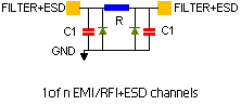
FEATURES 6 channels of EMI filtering with integrated ESD protection Pi-style EMI filters in a capacitor-resistor-capacitor (C-R-C) network Greater than 20dB attenuation (typical) at 1 GHz ±30kV ESD protection on each channel (HBM) ±15kV ESD protection on each channel (IEC 61000-4-2 Level 4, contact discharge) TDFN package with 0.40mm lead pitch,available with lead-free finishing. APPLICATIONS LCD and camera modules LCD and Camera data lines in mobile handsets I/O port protection for mobile handsets, notebook computers, PDAs etc. EMI filtering for data ports in cell phones, PDAs or notebook computers. Handheld PCs/PDAs Wireless handsets SHORT PRODUCT APPLICATION NOTE The SW1430 is a family of pi-style EMI filter arrays with ESD protection, which integrates four filters (C-R-C) in small form factor TDFN 0.40mm pitch packages. The SW1430 has component values of 8.5pF-100W-8.5pF per channel and a cut-off frequency of 200MHz. These integrated thin film resistor-networks can be used in applications where the data rates are as high as 80Mbps. The parts include ESD diodes on every pin, which providea very high level of protection for sensitive electronic components that may be subjected to electrostatic discharge (ESD). The ESD protection diodes safely dissipate ESD strikes of ±15kV, well beyond the maximum requirement of the IEC61000-4-2 international standard. Using the MIL-STD-883 (Method 3015) specification for Human Body Model (HBM) ESD, the pins are protected for contact discharges at greater than ±30kV. These devices are particularly well-suited for portable electronics (e.g. wireless handsets, PDAs, notebook computers) because of their small package and easy-to-use pin assignments.These products are manu factured using advanced thin film technologies including ultra-stable and self-passivating Tantalum Nitride resistors, gold interconnect metalization and reliable MNOS capacitors to achieve excellent uniformity, performance and reliability. In packaged form,TDFN packages where the pitch is 0.40mm ,these products are the best solution where space and weight are a concern. They are available with lead-free finishing. SEMICONDUCTOR-THIN FILM MANUFACTURING PROCESS DESCRIPTION Integrated passive networks are manufactured using advanced thin film technologies including ultra -stable and self passivating Tantalum Nitride resistors, gold interconnect metallization and reliable MNOS capacitors to achieve excellent uniformity, performance and reliability. Thin film resistor technology is the preferred solution for all applications that require low noise, long term stability and excellent performance at very high frequencies. Semiconwell employs proprietary thin film technologies for deposition of a wide range of sheet resistance films from 1 W/sq to 10,000 W/sq. All Semiconwell's products are available in die form and as KGD, known good die and are ideal for high reliability hybrid and multi chip module applications. Besides thin film resistors, Semiconwell integrates capacitors, Schottky diodes, Zener diodes and transistors. Integrated passive and active networks are manufactured using Semiconwell's in house high reliability semiconductor manufacturing processes. All semiconductor devices employ precision doping via ion implantation, silicon nitride junction passivation, platinum silicided contacts and gold interconnect metallization for best performance and reliability. MNOS capacitors and Tantalum Nitride resistors are easily integrated with Schottky diodes to provide complete standard and custom RCD solutions. In die form, these products are ideal for hybrid and multi chip module applications. In packaged form, these products are the best solution where space and weight are a concern. ABSOLUTE MAXIMUM RATINGS Storage Temperature Range -65 to 150 °C DC Power per Resistor 100 mW Package Power Rating 500 mW Stresses beyond listed absolute maximum ratings may cause permanent damage to the device. ELECTRICAL CHARACTERISTICS, Resistance min.80, typ. 100, max.120 W Operating Temperature Range -40 to 85 °C Total Channel Capacitance,At 2.5VDC Reverse Bias, 1MHz, 30mVAC min. 14, typ. 17, max.21 pF Capacitance C1, At 2.5VDC Reverse Bias, 1MHz, 30mVAC min. 7, typ. 8.5, max.11 pF Leakeage current (@25°C),V DIODE =±3.3V typ.0.1, max 1 µA Standoff Voltage,IDIODE =10 µA min. 5.5 V Signal Clamp Voltage, Positive Clamp,ILOAD =10 mA Negative Clamp,ILOAD =-10 mA min.5.6, typ.6.8, max.9 min.-1.5, typ.-0.8, max.-0.4 V V In-system ESD Withstand Voltage,Notes 2, 3 and 4 a) Human Body Model, MIL-STD-883, Method 3015 b) Contact Discharge per IEC 61000-4-2 Level 4 ±30 ±15 kV kV Dynamic Resistance Positive Negative typ. 2.3 typ. 0.9 W W Cut-off Frequency,ZSOURCE =50W,ZLOAD =50W,R=100W, C=30pF typ.200 MHz Note 1: T A =25°C unless otherwise specified. Note 2: ESD applied to input and output pins with respect to GND, one at a time. Note 3: Unused pins are left open Note 4: These parameters are guaranteed by design and characterization.


SEMICONWELL
Integrated Passive Networks
  ESD protected EMI Filter Network
SWPI1430-12


FEATURES
APPLICATIONS
SCHEMATIC
Six channels of EMI filtering with integrated ESD protection
Pi-style EMI filters in a capacitor-resistor-capacitor (C-R-C) network
Greater than 20dB attenuation (typical) at 1 GHz
±30kV ESD protection on each channel (HBM)
±15kV ESD protection on each channel (IEC 61000-4-2 Level 4, contact discharge)
 TDFN package with 0.40mm lead pitch,,available with lead-free finishing.
LCD and Camera data lines in mobile handsets
I/O port protection for mobile handsets, notebook computers, PDAs etc.
EMI filtering for data ports in cell phones, PDAs or notebook computers.
 Handheld PCs/PDAs
 Wireless handsets
 LCD and camera modules

SHORT PRODUCT APPLICATION NOTE
The SW1430 is a family of pi-style EMI filter arrays with ESD protection, which integrates four filters (C-R-C) in small form factor TDFN 0.40mm pitch packages. The SW1430 has component values of 8.5pF-100W-8.5pF per channel and a cut-off frequency of 200MHz. These integrated thin film resistor-networks can be used in applications where the data rates are as high as 80Mbps.. The parts include ESD diodes on every pin, which providea very high level of protection for sensitive electronic components that may be subjected to electrostatic discharge (ESD). The ESD protection diodes safely dissipate ESD strikes of ±15kV, well beyond the maximum requirement of the IEC61000-4- 2 international standard. Using the MIL-STD-883 (Method 3015) specification for Human Body Model (HBM) ESD, the pins are protected for contact discharges at greater than ±30kV. These devices are particularly well-suited for portable electronics (e.g. wireless handsets, PDAs, notebook computers) because of their small package and easy-to-use pin assignments.These products are manu factured using advanced thin film technologies including ultra-stable and self-passivating Tantalum Nitride resistors, gold interconnect metalization and reliable MNOS capacitors to achieve excellent uniformity, performance and reliability. In packaged form,TDFN packages where the pitch is 0.40mm ,these products are the best solution where space and weight are a concern.They are available with lead-free finishing.

SEMICONDUCTOR-THIN FILM MANUFACTURING PROCESS DESCRIPTION
Integrated passive networks are manufactured using advanced thin film technologies including ultra -stable and self passivating Tantalum Nitride resistors, gold interconnect metallization and reliable MNOS capacitors to achieve excellent uniformity, performance and reliability. Thin film resistor technology is the preferred solution for all applications that require low noise, long term stability and excellent performance at very high frequencies. Semiconwell employs proprietary thin film technologies for deposition of a wide range of sheet resistance films from 1 W/sq to 10,000 W/sq. All Semiconwell's products are available in die form and as KGD, known good die and are ideal for high reliability hybrid and multi chip module applications. Besides thin film resistors, Semiconwell integrates capacitors, Schottky diodes, Zener diodes and transistors. Integrated passive and active networks are manufactured using Semiconwell's in house high reliability semiconductor manufacturing processes. All semiconductor devices employ precision doping via ion implantation, silicon nitride junction passivation, platinum silicided contacts and gold interconnect metallization for best performance and reliability. MNOS capacitors and Tantalum Nitride resistors are easily integrated with Schottky diodes to provide complete standard and custom RCD solutions. In die form, these products are ideal for hybrid and multi chip module applications. In packaged form, these products are the best solution where space and weight are a concern.

ABSOLUTE MAXIMUM RATINGS

PARAMETER RATING UNITS
Storage Temperature Range
-65 to 150 °C
DC Power per Resistor
100 mW
Package Power Rating
500 mW

Stresses beyond listed absolute maximum ratings may cause permanent damage to the device.

ELECTRICAL CHARACTERISTICS, Note 1
PARAMETER VALUE UNITS
Resistance min.80, typ. 100, max.120 W
Operating Temperature Range -40 to 85 °C
Total Channel Capacitance,At 2.5VDC Reverse Bias, 1MHz, 30mVAC min. 14, typ. 17, max.21 pF
Capacitance C1, At 2.5VDC Reverse Bias, 1MHz, 30mVAC min. 7, typ. 8.5, max.11 pF
Leakeage current (@25°C),V DIODE =±3.3V typ.0.1, max 1 µA
Standoff Voltage,IDIODE =10 µA min. 5.5 V
Signal Clamp Voltage,
Positive Clamp,ILOAD =10 mA
Negative Clamp,ILOAD =-10 mA

min.5.6, typ.6.8, max.9
min.-1.5, typ.-0.8, max.-0.4

V
V
In-system ESD Withstand Voltage,Notes 2, 3 and 4
a) Human Body Model, MIL-STD-883, Method 3015
b) Contact Discharge per IEC 61000-4-2 Level 4

±30
±15

kV
kV
Dynamic Resistance
Positive
Negative

typ. 2.3
typ. 0.9 

W
W  
Cut-off Frequency,ZSOURCE =50W,ZLOAD =50W,R=100W, C=30pF typ.200   MHz
Note 1: T A =25°C unless otherwise specified.
Note 2: ESD applied to input and output pins with respect to GND, one at a time.
Note 3: Unused pins are left open
Note 4: These parameters are guaranteed by design and characterization.

GENERAL DIE INFORMATION
Substrate Thickness (mils) Die size (mils) Bonding pads Backside metal
SiO2 / Silicon 10±2 90 x 60 ±3 4x4 mils, 3mm thick, 99.99% electroplated gold with a TiW barrier Au/Si compatible with eutectic and conductive epoxy die attach.
All Semiconwell products are available in die form for chip and wire hybrid circuits and multi chip modules applications. Typical delivery for standard die products is 3-4 weeks ARO. For Chip Scale Packaged (CSP) devices consult factory for an update on availability of certain products.

DIODES RESISTORS CAPACITORS
The diodes offer basic ESD protection, with low forward voltage, low leakage and low power dissipation in OFF state. Resistive material is ultra stable TaN with low TCR <75ppm/°C typical. For Rsq<10W/sq and Rsq>500W/sq, the resistive material is proprietary. Power rating/resistor max 100mW for R<1KW and 25mW for R>1KW. Standard tolerance is ±5%. Silicon nitride dielectric, MNOS capacitors exhibit high stability, low temperature coefficients, low leakage <10nA and high BV>50V.

DIE/PACKAGE LAYOUT SCHEMATIC DIAGRAM
tdfn 12 lads
Top view, bottom pads in gray
swpi cm 1430 6 channels
Channel pairs=[1,12],[2,11],[3,10],[4,9],[5,8],[6,7]
Vss=die backside

STANDARD PRODUCTS ORDERING INFORMATION

TDFN-12 BARE DIE-12
SWPI1430-12TD SWPT1430-12BD

SW PART # QUANTITY TDFN-12 U/P($) BARE DIE U/P($)
SWPI1430-12   5,000pc -12TD    -12BD  
SWPI1430-12 10,000pc -12TD    -12BD  
For products sold as bare tested die or known good die KGD, minimum order is 5000pc. Dice are 100% functional tested, visual inspected and shipped in antistatic waffle packs. For special die level KGD requirements, different packaging or custom configurations, contact sw_sales@semiconwell.com

INSTANT QUOTE
Semiconwell P/N Quantity E-mail    
 

Delivery for packaged RCD standard products is 6-8 weeks ARO. Certain items may be available from stock. For standard products available from stock, there is a minimum line item order of $250.0. Inventory is periodically updated. For 2500pc or larger orders, all surface mount packaged devices are shipped in tape on reel (T/R). For smaller quantities, it may vary. Samples are available only for customers that have issued firm orders pending qualification of product in a particular application. On line Orders have to be verified, accepted and acknowledged by Semiconwell sales department in writing before, becoming non cancelable binding contracts.

Semiconwell guarantees continuous supply and availability of any of it's standard products provided minimum order quantities are met.

SEMICONWELL has made every effort to have this information as accurate as possible. However, no responsibility is assumed by SEMICONWELL for its use, nor for any infringements of rights of third parties which may result from its use. SEMICONWELL reserves the right to revise the content or modify its product line without prior notice. SEMICONWELL products are not authorized for and should not be used within support systems which are intended for surgical implants into the body, to support or sustain life, in aircraft, space equipment, submarine, or nuclear facility applications without the specific written consent.

Home Product Tree Tech. Support Print PDF Packages Request Quote Inventory Place Order Contact sales