ESD Protected RCR T Filter Network Suitable for I/O interface cards Multiple EMI/RFI protection lines/package Stable resistor-capacitor network Saves board space and component cost ESD protection > 2kV EMI/RFI Filters Low pass filters RS232 Serial Port Filter These integrated thin film resistor-networks is designed to suppress EMI/RFI noise at I/O ports of personal computers and peripherals, workstations, Local Area Network (LAN), Asynchronous Transfer Mode (ATM), Wide Area Network (WAN), etc. The filter includes ESD protection circuitry witch prevents device destruction when subjected to ESD discharges of up to 5kV. The ESD protection circuitry permits the filter to operate on bipolar signals of up to +12V. These products are integrated thin film resistor-networks that are designed to suppress transmission line effects on high-speed data lines. The TESD series solution improves performance and reduces assembly cost on passive components. These products are manufactured using advanced thin film technologies including ultra-stable and self-passivating Tantalum Nitride resistors, gold interconnect metalization and reliable MNOS capacitors to achieve excellent uniformity, performance and reliability. In die form, these products are ideal for hybrid and multi-chip module applications. In packaged form, these products are the best solution where space and weight are a concern.


SEMICONWELL
Integrated Passive Networks
  ESD Protected RCR T Filter Network
SWTESD XXX/XXX-24


FEATURES
APPLICATIONS
SCHEMATIC
Suitable for I/O interface cards
10 EMI/RFI protection lines/package
Stable resistor-capacitor network
Saves board space and component cost
ESD protection > 2kV
 
EMI/RFI Filters
Low pass filters
RS232 Serial Port Filter


schematic

SHORT PRODUCT APPLICATION NOTE
These integrated thin film resistor-networks is designed to suppress EMI/RFI noise at I/O ports of personal computers and peripherals, workstations, Local Area Network (LAN), Asynchronous Transfer Mode (ATM), Wide Area Network (WAN), etc. The filter includes ESD protection circuitry witch prevents device destruction when subjected to ESD discharges of up to 5kV. The ESD protection circuitry permits the filter to operate on bipolar signals of up to +12V. These products are integrated thin film resistor-networks that are designed to suppress transmission line effects on high-speed data lines. The TESD series solution improves performance and reduces assembly cost on passive components. These products are manufactured using advanced thin film technologies including ultra-stable and self-passivating Tantalum Nitride resistors, gold interconnect metalization and reliable MNOS capacitors to achieve excellent uniformity, performance and reliability. In die form, these products are ideal for hybrid and multi-chip module applications. In packaged form, these products are the best solution where space and weight are a concern.

SEMICONDUCTOR-THIN FILM MANUFACTURING PROCESS DESCRIPTION
Integrated passive networks are manufactured using advanced thin film technologies including ultra -stable and self passivating Tantalum Nitride resistors, gold interconnect metallization and reliable MNOS capacitors to achieve excellent uniformity, performance and reliability. Thin film resistor technology is the preferred solution for all applications that require low noise, long term stability and excellent performance at very high frequencies. Semiconwell employs proprietary thin film technologies for deposition of a wide range of sheet resistance films from 1 W/sq to 10,000 W/sq. All Semiconwell's products are available in die form and as KGD, known good die and are ideal for high reliability hybrid and multi chip module applications. Besides thin film resistors, Semiconwell integrates capacitors, Schottky diodes, Zener diodes and transistors. Integrated passive and active networks are manufactured using Semiconwell's in house high reliability semiconductor manufacturing processes. All semiconductor devices employ precision doping via ion implantation, silicon nitride junction passivation, platinum silicided contacts and gold interconnect metallization for best performance and reliability. MNOS capacitors and Tantalum Nitride resistors are easily integrated with Schottky diodes to provide complete standard and custom RCD solutions. In die form, these products are ideal for hybrid and multi chip module applications. In packaged form, these products are the best solution where space and weight are a concern.

MAXIMUM POWER RATINGS
100mW@70°C/channel 1000mW@70°C/package

Stresses beyond listed absolute maximum ratings may cause permanent damage to the device.

ELECTRICAL CHARACTERISTICS
PARAMETER VALUE UNITS
Absolute Tolerance R 1, 5, 10 %
Absolute Tolerance C 20 %
Operating Temperature Range 0 to70 °C
Storage Temperature Range -65 to 150 °C
Leakeage current (@25°C) max 1 µA
Crosstalk < 5 %
Signal Clamp Voltage
Positive Clamp
Negative Clamp

>+6
<-6
V
ESD protection >2 kV
* Guaranteed by design

GENERAL DIE INFORMATION
Substrate Thickness (mils) Die size (mils) Bonding pads Backside metal
SiO2 / Silicon 10±2 90 x 60 ±3 4x4 mils, 3mm thick, 99.99% electroplated gold with a TiW barrier Au/Si compatible with eutectic and conductive epoxy die attach.
All Semiconwell products are available in die form for chip and wire hybrid circuits and multi chip modules applications. Typical delivery for standard die products is 3-4 weeks ARO. For Chip Scale Packaged (CSP) devices consult factory for an update on availability of certain products.

DIODES RESISTORS CAPACITORS
Schottky diodes offer basic ESD protection, with low forward voltage, low leakage and low power dissipation in OFF state. Schottky Diodes exhibit low junction capacitance CTand low on resistance RDON. 
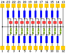
Resistive material is ultra stable TaN with low TCR <75ppm/°C typical. For Rsq<10W/sq and Rsq>500W/sq, the resistive material is proprietary. Power rating/resistor max 100mW for R<1KW and 25mW for R>1KW. Standard tolerance is ±5%. Silicon nitride dielectric, MNOS capacitors exhibit high stability, low temperature coefficients, low leakage <10nA and high BV>50V.

DIE/PACKAGE LAYOUT SCHEMATIC DIAGRAM
layout schematic
I/O=2-11,14-23
Vss=die backside
Vss=1,12,13,24
Vdd=2,7,10,15

STANDARD PRODUCTS ORDERING INFORMATION

R* (W) C** (pF) fc @3dB [MHz] QSOP-24 TQSOP-24 TSSOP-24 BARE DIE-24
10 15 1063 SWTESD/100/150-24QS SWTESD/100/150-24TQS SWTESD/100/150-24TS SWTESD/100/150-24BD
10 100 160 SWTESD/100/101-24QS SWTESD/100/101-24TQS SWTESD/100/101-24TS SWTESD/100/101-24BD
15 47 226 SWTESD/150/470-24QS SWTESD/150/470-24TQS SWTESD/150/470-24TS SWTESD/150/470-24BD
25 100 64 SWTESD/250/101-24QS SWTESD/250/101-24TQS SWTESD/250/101-24TS SWTESD/250/101-24BD
25 200 32 SWTESD/250/201-24QS SWTESD/250/201-24TQS SWTESD/250/201-24TS SWTESD/250/201-24BD
33 47 103 SWTESD/330/470-24QS SWTESD/330/470-24TQS SWTESD/330/470-24TS SWTESD/330/470-24BD
33 100 27 SWTESD/330/101-24QS SWTESD/330/101-24TQS SWTESD/330/101-24TS SWTESD/330/101-24BD
33 220 22 SWTESD/330/221-24QS SWTESD/330/221-24TQS SWTESD/330/221-24TS SWTESD/330/221-24BD
39 50 82 SWTESD/390/500-24QS SWTESD/390/500-24TQS SWTESD/390/500-24TS SWTESD/390/500-24BD
39 220 19 SWTESD/390/221-24QS SWTESD/390/221-24TQS SWTESD/390/221-24TS SWTESD/390/221-24BD
47 33 103 SWTESD/470/330-24QS SWTESD/470/330-24TQS SWTESD/470/330-24TS SWTESD/470/330-24BD
47 47 72 SWTESD/470/470-24QS SWTESD/470/470-24TQS SWTESD/470/470-24TS SWTESD/470/470-24BD
100 100 16 SWTESD/101/101-24QS SWTESD/101/101-24TQS SWTESD/101/101-24TS SWTESD/101/101-24BD
* Tolerance ±10%
** Tolerance ±20%

SW PART # QUANTITY QSOP-24 U/P($) TQSOP-24 U/P($) TSSOP-24 U/P($) BARE DIE U/P($)
SWTESD/RCCODE-10%   5,000pc -24QS   -24TQS   -24TS   -24BD  
SWTESD/RCCODE-10% 10,000pc -24QS   -24TQS   -24TS   -24BD  
SWTESD/RCCODE-5%      5,000pc -24QS   -24TQS   -24TS   -24BD  
SWTESD/RCCODE-5%    10,000pc -24QS   -24TQS   -24TS   -24BD  
SWTESD/RCCODE-1%      5,000pc -24QS   -24TQS   -24TS   -24BD  
SWTESD/RCCODE-1%    10,000pc -24QS   -24TQS   -24TS   -24BD  
For products sold as bare tested die or known good die KGD, minimum order is 5000pc. Dice are 100% functional tested, visual inspected and shipped in antistatic waffle packs. For special die level KGD requirements, different packaging or custom configurations, contact sw_sales@semiconwell.com

INSTANT QUOTE
Semiconwell P/N Quantity E-mail    
 

Delivery for packaged RCD standard products is 6-8 weeks ARO. Certain items may be available from stock. For standard products available from stock, there is a minimum line item order of $250.0. Inventory is periodically updated. For 2500pc or larger orders, all surface mount packaged devices are shipped in tape on reel (T/R). For smaller quantities, it may vary. Samples are available only for customers that have issued firm orders pending qualification of product in a particular application. On line Orders have to be verified, accepted and acknowledged by Semiconwell sales department in writing before, becoming non cancelable binding contracts.

Semiconwell guarantees continuous supply and availability of any of it's standard products provided minimum order quantities are met.

SEMICONWELL has made every effort to have this information as accurate as possible. However, no responsibility is assumed by SEMICONWELL for its use, nor for any infringements of rights of third parties which may result from its use. SEMICONWELL reserves the right to revise the content or modify its product line without prior notice. SEMICONWELL products are not authorized for and should not be used within support systems which are intended for surgical implants into the body, to support or sustain life, in aircraft, space equipment, submarine, or nuclear facility applications without the specific written consent.

Home Product Tree Tech. Support Print PDF Packages Request Quote Inventory Place Order Contact sales