Multiple channels live ESD protection up to 13KV EMI/RFI noise filter for high frequencies Serial port ESD protection Live ESD protection for printer port up to 13KV EMI/RFI noise filter for high frequencies ESD discharge during operation Integrated with VP terminal connected to the positive rail, e.g. +12V and the VN terminal connected to the negative rail, e.g. -12V, of a RS232 supply and the RS232 transmit and receive lines from the RS232 connector routed through the SWDN002, this IC will effectively protect the RS232 chips from ESD discharges up to 25KV (human body mode, 100pF through 1.5KW) which also includes prevention of ESD induced latch-up.


SEMICONWELL
Integrated Passive Networks
  CLAMP DIODE NETWORK
SWDN002-28


FEATURES
APPLICATIONS
SCHEMATIC
24 channels live ESD protection up to 13KV
EMI/RFI noise filter for high frequencies


Live ESD protection for printer port up to 13KV
Protection of IC terminals which are exposed to ESD discharge during operation
Serial port ESD protection


schematic
6, 14 - VSS, 22, 28 - VDD

SHORT PRODUCT APPLICATION NOTE
Integrated with VP terminal connected to the positive rail, e.g. +12V and the VN terminal connected to the negative rail, e.g. -12V, of a RS232 supply and the RS232 transmit and receive lines from the RS232 connector routed through the SWDN002, this IC will effectively protect the RS232 chips from ESD discharges up to 15KV (human body model, 100pF through 1.5KW) and 8kV per IEC61000-4-2. Also includes prevention of ESD induced latch-up.

SEMICONDUCTOR-THIN FILM MANUFACTURING PROCESS DESCRIPTION
Integrated passive networks are manufactured using advanced thin film technologies including ultra -stable and self passivating Tantalum Nitride resistors, gold interconnect metallization and reliable MNOS capacitors to achieve excellent uniformity, performance and reliability. Thin film resistor technology is the preferred solution for all applications that require low noise, long term stability and excellent performance at very high frequencies. Semiconwell employs proprietary thin film technologies for deposition of a wide range of sheet resistance films from 1W/sq to 10,000 W/sq. All Semiconwell's products are available in die form and as KGD, known good die and are ideal for high reliability hybrid and multi chip module applications. Besides thin film resistors, Semiconwell integrates capacitors, Schottky diodes, Zener diodes and transistors. Integrated passive and active networks are manufactured using Semiconwell's in house high reliability semiconductor manufacturing processes. All semiconductor devices employ precision doping via ion implantation, silicon nitride junction passivation, platinum silicided contacts and gold interconnect metallization for best performance and reliability. MNOS capacitors and Tantalum Nitride resistors are easily integrated with Schottky diodes to provide complete standard and custom RCD solutions. In die form, these products are ideal for hybrid and multi chip module applications. In packaged form, these products are the best solution where space and weight are a concern.

ABSOLUTE MAXIMUM RATINGS
Maximum Supply Voltage Maximum IF Max Power dissipation
12V 20mA 50mW@70°C/channel

Stresses beyond listed absolute maximum ratings may cause permanent damage to the device.

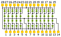
STANDARD SPECIFICATIONS
PARAMETER VALUE UNITS
Supply Voltage (VDD-VSS) -0.3...+12 V
DC voltage at any channel input (Vsignal) (VN-0.5) to (VP+0.5) V
Supply current Vp-Vn=12V max 10 µA
Diode forward voltage VF, IF=20mA, Ta=°C min 0.65 max 1 V
Channel Input capacitance @1 MHz, Vp=12V, VN=0, Vin=6V min 5.5 max 12 pF
Operating Temperature (TOP) -20 to 85 °C
Storage Temperature (Tstg) -65 to +150 °C
ESD Protection, Voltage at any channel input
Human Body Model, Method 3015 (Note 2,3)
Contact Discharge per IEC61000-4-2 (Note 4)

±15
±8

kV
kV
Channel clamp voltage under ESD test conditions (see above)
Positive Transients
Negative Transients

VP+13
VN-13

V
V
Channel Leakage(0<Vin<Vdd) typ 0.1 max. 10 µA
Operating Temperature (TOP) -20 to 85 °C
Storage Temperature (Tstg) -65 to +150 °C
 
Note1: Absolute maximum ratings for one diode conducting at a time.
Note2: From I/O pins to VP or VN only. Vp bypassed to VN with 0.2µF ceramic capacitor .
Note3: Human Body Model per MIL-STD-883, Method 3015 Cdischarge=100pF, Rdischarge=1.5kW, VP=12V, VN=0
Note4: This parameter guaranteed by characterisation.

GENERAL DIE INFORMATION
Substrate Thickness (mils) Die size (mils) Bonding pads Backside metal
SiO2 / Silicon 10±2 90 x 60 ±3 4x4 mils, 3mm thick, 99.99% electroplated gold with a TiW barrier Au/Si compatible with eutectic and conductive epoxy die attach.
All Semiconwell products are available in die form for chip and wire hybrid circuits and multi chip modules applications. Typical delivery for standard die products is 4-6 weeks ARO. For Chip Scale Packaged (CSP) devices consult factory for an update on availability of certain products.

DIODES BONDING PADS CAPACITORS
Junction diodes offers basic ESD protection, with low forward voltage and low power dissipation. Diodes are small physically resulting tipical load capacitance of 30 pF. The bonding pads are 3µm thick, 99.99% electroplated gold with a TiW barrier that withstands 30 min at 400°C in air without loss of adhesion. Silicon nitride dielectric, MNOS capacitors exhibit high stability, low temperature coefficients, low leakage <10nA and high BV>50V.

DIE / PACKAGE LAYOUT PACKAGE PIN OUT
layout schematic
14 - VSS, 28 - VDD
I/O=1-5,7-13,15-21,23-27
Vss=die backside
Vss=6,14
Vdd=22,24

STANDARD PRODUCTS ORDERING INFORMATION

PART# QSOP-28 TSSOP-28 BARE DIE
SWDN002 SWDN002-28QS SWDN002-28TS SWDN002-28BD

SW PART # QUANTITY QSOP-28 U/P($) TSSOP-28 U/P($) BARE DIE U/P($)
SWDN002   5,000pc -28QS   -28TS   -28BD  
SWDN002 10,000pc -28QS   -28TS   -28BD  
For custom products sold as bare tested die or known good die KGD, minimum order is 5000pc. Dice are 100% functional tested, visual inspected and shipped in antistatic waffle packs. For special die level KGD requirements, different packaging or custom configurations, contact sw_sales@semiconwell.com

  Semiconwell P/N Quantity E-mail    
Receive Instant Quote
 

Delivery for packaged RCD standard products is 6-8 weeks ARO. Certain items may be available from stock. For standard products available from stock, there is a minimum line item order of $250.0. Inventory is periodically updated. For 2500pc or larger orders, all surface mount packaged devices are shipped in tape on reel (T/R). For smaller quantities, it may vary. Samples are available only for customers that have issued firm orders pending qualification of product in a particular application. On line Orders have to be verified, accepted and acknowledged by Semiconwell sales department in writing before, becoming non cancelable binding contracts.

Semiconwell guarantees continuous supply and availability of any of it's standard products provided minimum order quantities are met.

SEMICONWELL has made every effort to have this information as accurate as possible. However, no responsibility is assumed by SEMICONWELL for its use, nor for any infringements of rights of third parties which may result from its use. SEMICONWELL reserves the right to revise the content or modify its product line without prior notice. SEMICONWELL products are not authorized for and should not be used within support systems which are intended for surgical implants into the body, to support or sustain life, in aircraft, space equipment, submarine, or nuclear facility applications without the specific written consent.

Home Product Tree Tech. Support Print PDF Packages Request Quote Inventory Place Order Contact sales