|
PACVGA200, PAC VGA200 same as SWVGA200 VGA PORT ESD PROTECTED TERMINATION, The SWVGA-200 incorporates 7 channels of ESD protection for signal lines commonly found in a VGA port
VGA PORT ESD PROTECTED TERMINATION SWVGA-200
FEATURES APPLICATIONS SCHEMATIC
7 channels of ESD protection for all VGA port connector pins meeting IEC-1000-4-2 Level-4 ESD requirements (8KV contact discharge) ESD protection for VGA (video) port in PCs and notebooks.
Very low loading capacitance from ESD protection diodes, 4pF typical
TTL to CMOS level-translating buffers for the HSYNC and VSYNC lines
75 W retmination resistors for VIDEO lines (matched to 1% typ.)
Bi-directional level shifting N-channel FETs provided for DDC_CLK&DDC_DATA channels
SHORT PRODUCT APPLICATION NOTE
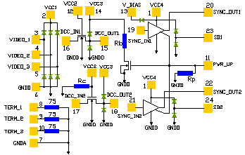
The SWVGA-200 incorporates 7 channels of ESD protection for signal lines commonly found in a VGA port . ESD protection is implemented with current steering diodes designed to safely handle the high peak surge currents associated with the IEC-1000-4-2 Level-4 ESD Protection Standard (8KV contact discharge). When a channel is subjected to an electrostatic discharge, the ESD current pulse is diverted via the protection diodes into the positive supply rails or ground where they may be safely dissipated. Separate positive supply rails are provided for the VIDEO,DDC and SYNC channels to facilitate interfacing with low voltage Video Controller ICs and provide design flexibility in multi-suply-voltage environments. Two non-inverting drivers provide buffering for the HSYNC and VSYNC channels from the Video Controller IC(SYNC1,SYNC2).These buffers accept TTL input levels and convert them to CMOS output levels that swing between Ground and VCC4.These drivers have nominal 60W otput impedance to match the characteristic impedance of the HSYNC&VSYNC lines of the video cables typically used in PC applications. Two N-channel FETs provide the level shifting function required when the DDC controller is operated at a lower supply voltae than the monitor. Three 75W termination resistors suitable for terminating the video signals from the video DAC are also provided. Thee resistors have separated input pins to allow insertion of additional EMI filtering, if required, between the termination point and the ESD protection diodes. These resistors are matched to better than 2% for excellent signal level matching for the R/G/B signals. When the PWR_UP input is driven LOW the SYNC inputs can be floated without causing the SYNC buffers to draw any current from the VCC3 supply. When the PWR_UP input is LOW the SYNC outputs are driven LOW. An internal diode (D1 in schematic below) is also provided so that VCC4 can be derived from VCC4, if desired, by connecting VCC3 to V_BIAS. In applications where VCC4 may be powered down, diode D1 blocks any DC current path from the DDC_OUT pins back to the powered down VCC4 rail via the top ESD protection diodes.
SEMICONDUCTOR-THIN FILM MANUFACTURING PROCESS DESCRIPTION
Integrated passive networks are manufactured using advanced thin film technologies including ultra -stable and self passivating Tantalum Nitride resistors, gold interconnect metallization and reliable MNOS capacitors to achieve excellent uniformity, performance and reliability. Thin film resistor technology is the preferred solution for all applications that require low noise, long term stability and excellent performance at very high frequencies. Semiconwell employs proprietary thin film technologies for deposition of a wide range of sheet resistance films from 1W/sq to 10,000 W/sq. All Semiconwell's products are available in die form and as KGD, known good die and are ideal for high reliability hybrid and multi chip module applications. Besides thin film resistors, Semiconwell integrates capacitors, Schottky diodes, Zener diodes and transistors. Integrated passive and active networks are manufactured using Semiconwell's in house high reliability semiconductor manufacturing processes. All semiconductor devices employ precision doping via ion implantation, silicon nitride junction passivation, platinum silicided contacts and gold interconnect metallization for best performance and reliability. MNOS capacitors and Tantalum Nitride resistors are easily integrated with Schottky diodes to provide complete standard and custom RCD solutions. In die form, these products are ideal for hybrid and multi chip module applications. In packaged form, these products are the best solution where space and weight are a concern.
ABSOLUTE MAXIMUM RATINGS
Reverse voltage VR Continuous IF IFRM for tw<100ms Max Power dissipation
7V 100mA 200 mA (20%duty cycle) 100mW@70°C/channel
Stresses beyond listed absolute maximum ratings may cause permanent damage to the device.
ABSOLUTE MAXIMUM RATINGS
PARAMETER VALUE UNITS
VCC1,VCC2,VCC3&VCC4 supply voltage GND-0.5, 6.0 V
Diode D1 Forward Current 100 µA
DC Voltage at Inputs VIDEO_1,VIDEO_2,VIDEO_3 GND -0.5, VCC1 +0.5 V
DC Voltage at Inputs ,TERM_1,TERM_2,TERM_3 -6.6, +6.0 V
DC Voltage at Inputs ,DDC_IN1,DDC_IN2 GND -0.5, VCC2 +0.5 V
DC Voltage at Inputs ,DDC_OUT1,DDC_OUT2 GND -0.5, VCC3 +0.5 V
DC Voltage at Inputs ,SYNC_IN1,SYNC_IN2 GND -0.5, VCC4 +0.5 V
Storage Temperature -40 to 150 °C
Operating Ambient Temperature 0 to 70 °C
Package Power Dissipation <1.0 W
ELECTRICAL CHARACTERISTICS
PARAMETER VALUE UNITS
VCC1 supply current , VCC1=5V; VIDEO inputs at VCC1 or GND 10(max.) mA
VCC2 ,VCC3 supply current, VCC2=VCC3=5V 10(max.) mA
VCC4 supply current , VCC4=5V;SYNC inputs at GND or VCC4; PWR_UP pin at VCC4; SYNC outputs unloaded 10(typ.) mA
VCC4 supply current , VCC4=5V;SYNC inputs at 3.0V; PWR_UP pin at VCC4; SYNC outputs unloaded 200(typ.) mA
VCC4 supply current , VCC4=5V;PWR_UP pin at GND; SYNC outputs unloaded 10(max.) mA
VBIAS open circuit voltage, No external current drawn from VBIAS pin VCC4-0.8(typ.) V
VIDEO termination resistance 71.25(min.) 75(typ.) 78.75(max.) W
RT resistance matching 1(typ.);2(max.)
Logic high input voltage (Note 1); VCC4=5.0V 2.0(min.) V
Logic low input voltage (Note 1); VCC4=5.0V 0.8(max.) V
Logic high output voltage (Note 1); VCC4=5.0V;IO=-4mA 4.4(min.) V
Logic low output voltage (Note 1); VCC4=5.0V;IO=4mA 0.4(max.) V
Resistor value; PWR_UP, VCC3=5.0V 0.5(min.)1(typ.)2(max.) MW
VCC2 pull-down resistor;VCC2=3.0V 0.5(min.)1.5(typ.)3(max.) MW
Input current; VIDEO inputs;VCC1=5.0V; VIN=VCC1or GND 1(max.) µA
Input current;HSYNC,VSYNC inputs;VCC4=5.0V; VIN=VCC4or GND 1(max.) µA
ON state leakage current, level shifting NFET; VCC2=VDDC_IN-0.4;VDDC_OUT=VCC2 10(max.) µA
ON state leakage current, level shifting NFET; VCC2=VDDC_OUT-0.4;VDDC_IN=VCC2 10(max.) µA
Voltage drop across level shifting NFET when turned ON; VCC2=2.5V; VS=GND,IDS=3mA 0.15(max.) V
Input capacitance (Note 3) VIDEO_1,VIDEO_2,VIDEO_3;VCC1=5.0V; VIN=2.5V; measured at 1M 4.0(typ.) pF
Input capacitance (Note 3) VIDEO_1,VIDEO_2,VIDEO_3;VCC1=2.5V; VIN=1.25V; measured at 1M 4.5(typ.) pF
SYNC drivers L-H propagation delay;CL=50 pF; VCC3=5V; Input tf and tf_5ns 8(typ.) 12(max.) ns
SYNC drivers H-L propagation delay;CL=50 pF; VCC3=5V; Input tf and tf_5ns 8(typ.) 12(max.) ns
SYNC drivers output rise&fall times;CL=50 pF; VCC3=5V; Input tf and tf_5ns 7(typ.) ns
ESD withstand voltage (Note 2,3) VCC1=VCC3=VCC4=5V 8(min.) KV
Note 1: These parameters apply only to the HSYNC and VSYNC channels. Note.2 Per the IEC-1000-4-2 ESD Standard, Level 4 contact discharge method. VCC1, VCC3 and VCC4 must be bypassed to GND via a low impedance ground plane with a 0.2µF, low impedance , chip ceramic capacitor at each supply pin. ESD pulse is applied between the applicable pins and GND.ESD pulse can be positive or negative with respect to GND. Applicable pins are: VIDEO_1,VIDEO_2,VIDEO_3,SYNC_OUT1,SD1,SYNC_OUT2,SD2,DDC_OUT1 and DDC_OUT2. All other pins are ESD protected to industry standard 2KV per the Human Body Model (MIL-STD-883, Method 3015). Note 3.This parameter in guaranteed by design and characterization.
PIN DESCRIPTION
LEAD NAME
1 VCC4
2 VCC1
3 VIDEO_1
4 VIDEO_2
5 VIDEO_3
6 GNDD
7 GNDA
8 TERM_1
9 TERM_2
10 TERM_3
11 POWER_UP
12 VCC2
13 V_BIAS
14 VCC3
15 DDC_OUT1
16 DDC_IN1
17 DDC_IN2
18 DDC_OUT2
19 SYNC_IN1
20 SYNC_OUT1
21 SYNC_IN2
22 SYNC_OUT2
23 SD1
24 SD2
GENERAL DIE INFORMATION
Substrate Thickness (mils) Die size (mils) Bonding pads Backside metal
SiO2 / Silicon 10±2 90 x 60 ±3 4x4 mils, 3mm thick, 99.99% electroplated gold with a TiW barrier Au/Si compatible with eutectic and conductive epoxy die attach.
All Semiconwell products are available in die form for chip and wire hybrid circuits and multi chip modules applications. Typical delivery for standard die products is 3-4 weeks ARO. For Chip Scale Packaged (CSP) devices consult factory for an update on availability of certain products.
DIODES RESISTORS CAPACITORS
Diodes offers basic ESD protection, with low forward voltage and low power dissipation. Diodes are small physically resulting low junction capacitance and low loading capacitance. Resistive material is ultra stable TaN with low TCR <75ppm/°C typical. For Rsq<10W/sq and Rsq>500W/sq, the resistive material is proprietary. Power rating/resistor max 100mW for R<1KW and 25mW for R>1KW. Standard tolerance is ±5%. Silicon nitride dielectric, MNOS capacitors exhibit high stability, low temperature coefficients, low leakage <10nA and high BV>50V.
DIE LAYOUT PACKAGE PIN OUT
Vin=3,4,5,6,11,12,13,14
Vss=die backside
Vss=1,8,9,16
Vdd=2,7,10,15
STANDARD PRODUCTS ORDERING INFORMATION
SOIC-24 QSOP-24 BARE DIE-24
SWVGA200-24SO SWVGA200-24QS SWVGA200-24BD
SW PART # QUANTITY QSOP-24 U/P($) BARE DIE U/P($)
SWVGA200 5,000pc -24QS -24BD
SWVGA200 10,000pc -24QS -24BD
For products sold as bare tested die or known good die KGD, minimum order is 5000pc. Dice are 100% functional tested, visual inspected and shipped in antistatic waffle packs. For special die level KGD requirements, different packaging or custom configurations, contact sw_sales@semiconwell.com
Delivery for packaged RCD standard products is 6-8 weeks ARO. Certain items may be available from stock. For standard products available from stock, there is a minimum line item order of $250.0. Inventory is periodically updated. For 2500pc or larger orders, all surface mount packaged devices are shipped in tape on reel (T/R). For smaller quantities, it may vary. Samples are available only for customers that have issued firm orders pending qualification of product in a particular application. On line Orders have to be verified, accepted and acknowledged by Semiconwell sales department in writing before, becoming non cancelable binding contracts.
Semiconwell guarantees continuous supply and availability of any of it's standard products provided minimum order quantities are met.
SEMICONWELL has made every effort to have this information as accurate as possible. However, no responsibility is assumed by SEMICONWELL for its use, nor for any infringements of rights of third parties which may result from its use. SEMICONWELL reserves the right to revise the content or modify its product line without prior notice. SEMICONWELL products are not authorized for and should not be used within support systems which are intended for surgical implants into the body, to support or sustain life, in aircraft, space equipment, submarine, or nuclear facility applications without the specific written consent.
|