|
CSPST8-16 same as SWST8-CSP 8 ISOLATED RESISTORS pin to pin compatible CHIP SCALE PACKAGE TERMINATION ARRAY
FEATURES 8 isolated high frequency series termination resistor in a single package 16-bump and 32-bump Chip Scale Packages (CSP) CSP package minimizes cross-talk 0.35 mm Eutectic Solder Bumps, 0.65 mm Pitch Ceramic substrate
Ultra small foot print package suitable for portable devices
APPLICATIONS Series resistive bus termination Servers High speed computing systems Notebook PCs Handheld devices Digital cameras and camcorders
SHORT PRODUCT APPLICATION NOTE
The SWST8-CSP is a high performance integrated Passive Device which provides series terminations suitable for use in high speed applications. Eight series termination channels are provided . These resistors provide excellent high frequency performance in excess of 3 GHz and are manufactured to an absolute tolerance of ±1%. The Chip Scale Package provides an ultra small footprint for this Integrated Passive Devices and provides minimal parasitics compared toconventional packaging. Typical bumps inductance is less than 25pH. The large solder bumps and ceramic substrate allow for standard attachment to laminate printed circuit boards without the use of underfill.
SEMICONDUCTOR-THIN FILM MANUFACTURING PROCESS DESCRIPTION
Integrated passive networks are manufactured using advanced thin film technologies including ultra -stable and self passivating Tantalum Nitride resistors, gold interconnect metallization and reliable MNOS capacitors to achieve excellent uniformity, performance and reliability. Thin film resistor technology is the preferred solution for all applications that require low noise, long term stability and excellent performance at very high frequencies. Semiconwell employs proprietary thin film technologies for deposition of a wide range of sheet resistance films from 1 W/sq to 10,000 W/sq. All Semiconwell's products are available in die form and as KGD, known good die and are ideal for high reliability hybrid and multi chip module applications. Besides thin film resistors, Semiconwell integrates capacitors, Schottky diodes, Zener diodes and transistors. Integrated passive and active networks are manufactured using Semiconwell's in house high reliability semiconductor manufacturing processes. All semiconductor devices employ precision doping via ion implantation, silicon nitride junction passivation, platinum silicided contacts and gold interconnect metallization for best performance and reliability. MNOS capacitors and Tantalum Nitride resistors are easily integrated with Schottky diodes to provide complete standard and custom RCD solutions. In die form, these products are ideal for hybrid and multi chip module applications. In packaged form, these products are the best solution where space and weight are a concern.
RESISTOR SPECIFICATIONS
Capacitance [pF] Tolerance q [%] Power Rating [mW]
<0.20pF 1, 5, 10 100 mW@70°C
Stresses beyond listed absolute maximum ratings may cause permanent damage to the device.
ELECTRICAL CHARACTERISTICS
PARAMETER VALUE UNITS
Resistor Tolerance ±1.0 %
MaximumResistor Power,at 70°C 0.1 W
Temperature Coefficient of Resistance ±100 ppm/°C
Storage Temperature Range -65°C to +150 °C
Operating Temperature Range -40°C to +85 °C
GENERAL DIE INFORMATION
Substrate Thickness (mils) Die size (mils) Bonding pads Backside metal
Al2O3 99.6 % 15±2 228x96±3 4x4 mils, 3mm thick, 99.99% electroplated gold with a TiW barrier Au/Si compatible with eutectic and conductive epoxy die attach.
All Semiconwell products are available in die form for chip and wire hybrid circuits and multi chip modules applications. Typical delivery for standard die products is 3-4 weeks ARO. For Chip Scale Packaged (CSP) devices consult factory for an update on availability of certain products.
CONDUCTORS RESISTORS BACKSIDE METAL
0.35mm Dia. Bumps Resistive material is ultra stable TaN with low TCR <75ppm/°C typical. For Rsq<10W/sq and Rsq>500W/sq, the resistive material is proprietary. Power rating/resistor max 100mW for R<1KW and 25mW for R>1KW. Standard tolerance is ±5%.
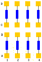
DIE LAYOUT PACKAGE PIN OUT
STANDARD PRODUCTS ORDERING INFORMATION
R R multiplier TOLERANCE
R value 22 24 27 30 33 36 39 43 47 51 56 R multiplier 1 -5% -1%
Find part #
SW PART # QUANTITY CSP-8 U/P($) BARE DIE U/P($)
SWST8/RCODE-5% 5,000pc -CSP8 -BD
SWST8/RCODE-5% 10,000pc -CSP8 -BD
For custom products sold as bare tested die or known good die KGD, minimum order is 5000pc. Dice are 100% functional tested, visual inspected and shipped in antistatic waffle packs. For special die level KGD requirements, different packaging or custom configurations, contact sw_sales@semiconwell.com
INSTANT QUOTE
Semiconwell P/N Quantity E-mail
Delivery for packaged Resistor networks standard products is 4-6 weeks ARO. Certain items may be available from stock. For standard products available from stock, there is a minimum line item order of $250.0. Inventory is periodically updated. For 2500pc or larger orders, all surface mount packaged devices are shipped in tape on reel (T/R). For smaller quantities, it may vary. Samples are available only for customers that have issued firm orders pending qualification of product in a particular application. On line Orders have to be verified, accepted and acknowledged by Semiconwell sales department in writing before, becoming non cancelable binding contracts.
|