|
SW1402 same as CM1402 manufactured by Semiconwell SIM CARD EMI FFILTER ARRAY WITH ESD PROTECTION CHIP SCALE SILICON
SIM Card EMI Filter Array with ESD Protection, CHIP SCALE SILICON SW1402-CSP
FEATURES APPLICATIONS
Three channels of EMI filtering, each with ESD protection SIM Card slot in mobile handsets
Two additional channels of ESD-only protection EMI filtering for data ports in cell phones, PDAs or notebook computers
±10kV ESD protection (IEC 61000-4-2, contact discharge) on all pins I/O port protection for mobile handsets, notebook computers, PDAs, etc.
±25kV ESD protection (HBM). Greater than 30dB of attenuation at 1GHz. 10-bump, 1.960mm x 1.330mm footprint Chip Scale Package (CSP)
SHORT PRODUCT APPLICATION NOTE
Many portable applications frequentely demand filtering of signals in the 800-2,700 MHz band. Semiconwell's thin film Flip Chip filters provide a minimum of -30dB of attenuation over this frequency band. The bump size and pitch of these filters are selected such that the device can be placed directly on a FR4 printed circuit board using conventional assembly techniques. Ground-bounce and cross-talk are minimum via a die design that provides two solder bump contacts to the common suply connection. The solder bumps are a 63/37 Sn/Pb alloy and are nominally 0.35 mm in diameter.The parts include avalanchetype ESD diodes on every pin, which provide a very high level of protection for sensitive electronic components that may be subjected to electrostatic discharge (ESD). The ESD diodes connected to the filter ports are designed and characterized to safely dissipate ESD strikes of ±10kV, beyond the maximum requirement of the IEC 61000-4-2 international standard. Using the MIL-STD-883 (Method 3015) specification for Human Body Model (HBM) ESD, the pins are protected for contact discharges at greater than ±25kV.
SEMICONDUCTOR-THIN FILM MANUFACTURING PROCESS DESCRIPTION
Integrated passive networks are manufactured using advanced thin film technologies including ultra -stable and self passivating Tantalum Nitride resistors, gold interconnect metallization and reliable MNOS capacitors to achieve excellent uniformity, performance and reliability. Thin film resistor technology is the preferred solution for all applications that require low noise, long term stability and excellent performance at very high frequencies. Semiconwell employs proprietary thin film technologies for deposition of a wide range of sheet resistance films from 1 W/sq to 10,000 W/sq. All Semiconwell's products are available in die form and as KGD, known good die and are ideal for high reliability hybrid and multi chip module applications. Besides thin film resistors, Semiconwell integrates capacitors, Schottky diodes, Zener diodes and transistors. Integrated passive and active networks are manufactured using Semiconwell's in house high reliability semiconductor manufacturing processes. All semiconductor devices employ precision doping via ion implantation, silicon nitride junction passivation, platinum silicided contacts and gold interconnect metallization for best performance and reliability. MNOS capacitors and Tantalum Nitride resistors are easily integrated with Schottky diodes to provide complete standard and custom RCD solutions. In die form, these products are ideal for hybrid and multi chip module applications. In packaged form, these products are the best solution where space and weight are a concern.
RESISTOR SPECIFICATIONS Capacitance 5pF Tolerance 10% Power Rating [mW] 25mW@70°C
Stresses beyond listed absolute maximum ratings may cause permanent damage to the device.
ELECTRICAL CHARACTERISTICS,Note 1
PARAMETER VALUE UNITS
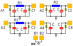
Resistor R1=100;R2=47 ohms
Absolute Tolerance, R ±10 %
Capacitor 20 pF
Absolute Tplerance, C ±20 %
TCR of Resistor ±100 ppm
Operating Temperature range -40 to +85 °C
Leakage Current@BIAS 3.3V max.1 mA
Power Rating/Resistor 25 mW
Stand-off Voltage ,I = 10µA typ.6.0 V
Signal Voltage,Positive Clamp,ILOAD = 10mA min.5.6, typ.6.8, max.9 V
Signal Voltage,Negative Clamp,ILOAD = -10mA min.-1.5,typ.-0.8,max.-0.4 V
In-system ESD Withstand Voltage,Human Body Model, MIL-STD-883,Method 3015,Notes 2,4 and 5 min.± 15 KV
In-system ESD Withstand Voltage,b) Contact Discharge per IEC,61000-4-2,Notes 2,4 and 5 min.± 10 KV
Clamping Voltage during ESD Discharge MIL-STD-883 (Method 3015),8kV Positive Transients,Notes 2,3,4 and 5 max.+12 V
Clamping Voltage during ESD Discharge MIL-STD-883 (Method 3015),8kV Negative Transients,Notes 2,3,4 and 5 max.-7 V
Cut-off frequency ZSOURCE = 50W, ZLOAD = 50W,R = 100W, C = 20pF 77 MHz
Cut-off frequency ZSOURCE = 50W, ZLOAD = 50W,R = 47W, C = 20pF 85 MHz
Note 1: TA=25°C unless otherwise specified. Note 2: ESD applied to input and output pins with respect to GND, one at a time. Note 3: Clamping voltage is measured at the opposite side of the EMI filter to the ESD pin. For example, if ESD is applied to Pin A1,then clamping voltage is measured at Pin C1. Note 4: Unused pins are left open Note 5: The parameters are guaranteed by design.
GENERAL DIE INFORMATION
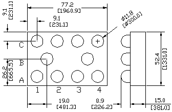
Substrate Thickness (mils) Die size (mils) Bonding pads
Si / Silicon 15±2 77 x 52±3 pure tin Sn or SnPb solder
All Semiconwell products are available in die form for chip and wire hybrid circuits and multi chip modules applications. Typical delivery for standard die products is 3-4 weeks ARO. For Chip Scale Packaged (CSP) devices consult factory for an update on availability of certain products.
CONDUCTORS RESISTORS BACKSIDE METAL not applicable
0.35 diameter bumps 63/37 Sn/Pb (Eutectic) or 96.8/2.6/0.6 Sn/Ag/Cu (Lead-free) solder bumps. Resistive material is ultra stable TaN with low TCR <75ppm/°C typical. For Rsq<10W/sq and Rsq>500W/sq, the resistive material is proprietary. Power rating/resistor max 100mW for R<1KW and 25mW for R>1KW. Standard tolerance is ±5%.
|