|
SWPIEMI1426-04 Same as CM1426-04, 4 CHANNEL LCD AND CAMERA EMI FILTER ARRAY WITH ESD PROTECTION
4 CHANNEL LCD AND CAMERA EMI FILTER ARRAY WITH ESD PROTECTION
SWPIEMI1426-04-CSP
FEATURES
APPLICATIONS
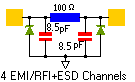
SCHEMATIC
Four channels of Pi-style EMI filtering, each with ESD protection
Greater than 20dB attenuation over the 800MHz to 3GHz.
±8kV ESD protection (IEC 61000-4-2, contact discharge)
±15kV ESD protection on each channel (HBM)
0.5mm pitch, 10-bump, 1.96mm x 1.33mm footprint.Chip Scale Package(CSP) . Chip Scale Package features extremely low lead inductance for optimum filter and ESDperformance
LCD and Camera data lines in mobile handsets
EMI filtering for data ports in cell phones, PDAs or
notebook computers
I/O port protection for mobile handsets, notebook
computers, PDAs etc.
EMI filtering for LCD and chip-to-chip data lines in mobile electronic devices that use flexible PCB
interconnections
SHORT PRODUCT APPLICATION NOTE
SWPIEMI1426 is a low-pass filter array integrating 4,6 or 8 pi-style filters (C-R-C) that reduce EMI/RFI emissions while at the same time providing ESD protection. Each high quality filter provides more than 20dB attenuation in the 800-3000 MHz range. In addition, the SWPIEMI1426 provides a very high level of protection for sensitive electronic components that may be subject to electrostatic discharge (ESD). The input pins are designed and characterized to safely dissipate ESD strikes of 8kV, the maximum requirement of the IEC 61000-4-2 international standard. Using the MIL-STD-883 (Method 3015) specification for Human Body Model (HBM) ESD, the device provides protection for contact discharges to greater than 15kV. The SWPIEMI1426 is particularly well suited for portable electronics (e.g., cellular telephones, PDAs, notebook computers) because of its small package format and low weight.In particular, the SWPIEMI1426 is ideal for EMI filtering and protecting data and control lines for the I/O data ports, LCD display and camera interface in mobile handsets.
SEMICONDUCTOR-THIN FILM MANUFACTURING PROCESS DESCRIPTION
Integrated passive networks are manufactured using advanced thin film technologies including ultra -stable and self passivating Tantalum Nitride resistors, gold interconnect metallization and reliable MNOS capacitors to achieve excellent uniformity, performance and reliability. Thin film resistor technology is the preferred solution for all applications that require low noise, long term stability and excellent performance at very high frequencies. Semiconwell employs proprietary thin film technologies for deposition of a wide range of sheet resistance films from 1W/sq to 10,000 W/sq. All Semiconwell's products are available in die form and as KGD, known good die and are ideal for high reliability hybrid and multi chip module applications. Besides thin film resistors, Semiconwell integrates capacitors, Schottky diodes, Zener diodes and transistors. Integrated passive and active networks are manufactured using Semiconwell's in house high reliability semiconductor manufacturing processes. All semiconductor devices employ precision doping via ion implantation, silicon nitride junction passivation, platinum silicided contacts and gold interconnect metallization for best performance and reliability. MNOS capacitors and Tantalum Nitride resistors are easily integrated with Schottky diodes to provide complete standard and custom RCD solutions. In die form, these products are ideal for hybrid and multi chip module applications. In packaged form, these products are the best solution where space and weight are a concern.
ABSOLUTE MAXIMUM RATINGS
Reverse voltage VR Continuous IF IFRM for tw<100ms Max Power dissipation
7V 100mA 200 mA (20%duty cycle) 100mW@70°C/channel
Stresses beyond listed absolute maximum ratings may cause permanent damage to the device.
ELECTRICAL CHARACTERISTICS
PARAMETER VALUE UNITS
Storage Temperature Range -65 to +150 °C
Operating Temperature Range -40 to +85 °C
DC Power per Resistor 100 mW
DC Package Power Rating 500 mW
Resistance Tolerance max.±20 %
Total Channel Capacitance,2.5VDC Reverse Bias, 1MHz, 30mVAC min.13.6,typ.17,max.20.4 pF
Capacitance C,2.5VDC Reverse Bias, 1MHz, 30mVAC min.6.8,typ.8.5,max.10.2 pF
Signal Voltage ,ILOAD = 10mA,Positive Clamp
Signal Voltage,ILOAD = -10mA,Negative Clamp
min.5.6 ; typ.6.8; max.9
min.-1.5;typ.-0.8;max.-0.4
V
V
In-system ESD Withstand Voltage,Notes 2,4 and 5
a) Human Body Model, MIL-STD-883,Method 3015
b) Contact Discharge per IEC 61000-4-2 Level 4
min.±15
min.±8
kV
kV
Dynamic Resistance
Positive
Negative
typ. 2.3
typ. 0.9
W
W
Cut-off frequency ; R = 100W, CTOTAL = 17pF,Note 6 typ.230 MHz
Diode Standoff Voltage,IDIODE = 10µA typ.6 V
Diode Leakage Current (reverse bias),VDIODE = 3.3V typ.0.1,max.1 µA
Note 1: TA =25°C unless otherwise specified
Note 2: ESD applied to input and output pins with respect to GND, one at a time.
Note 3: Clamping voltage is measured at the opposite side of the EMI filter to the ESD pin.
Note 4: Unused pins are left open
Note 5: The parameters are guaranteed by design and characterization.
Note 6: ZSOURCE=50W, ZLOAD=50W.
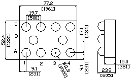
GENERAL DIE INFORMATION
Substrate Thickness (mils) Die size (mils) Bonding pads Backside metal
SiO2 / Silicon 15±2 77.2 x 52.4±3 0.30 DIA.
63/37 Sn/Pb (Eutectic)or 96.8/2.6/0.6 Sn/Ag/Cu (Lead-free)SOLDER BUMPS
All Semiconwell products are available in die form for chip and wire hybrid circuits and multi chip modules applications. Typical delivery for standard die products is 3-4 weeks ARO. For Chip Scale Packaged (CSP) devices consult factory for an update on availability of certain products.
DIODES RESISTORS CAPACITORS
The diodes offer basic ESD protection, with low forward voltage, low leakage and low power dissipation in OFF state.Diodes exhibit low junction capacitance CTand low on resistance RDON. Ultra stable TaN with low TCR <75ppm/°C typical. For Rsq<10W/sq and Rsq>500W/sq, resistive material is proprietary. Power rating/resistor max 100mW for R<1KW and 25mW for R>1KW. Standard tolerance is ±5%. Silicon nitride dielectric, MNOS capacitors exhibit high stability, low temperature coefficients, low leakage <10nA and high BV>50V.
|