|
PLCDA05 same as SWPLCDA05 ULTRA LOW CAPACITANCE TVS ARRAY
ULTRA LOW CAPACITANCE TVS ARRAY
SWPLCDA05
FEATURES
APPLICATIONS
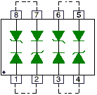
SCHEMATIC
500 Watts Peak Pulse Power per Line (tp=8/20 s)
Bidirectional configuration
IEC Compatibility:
61000-4-2(ESD)-Air 15KV,Contact 8KV;
61000-4-4 (EFT) 40A-5/50ns
61000-4-5 (Surge) 24A-8/20µs Level 2 (line-ground) Level 3 (line-line)
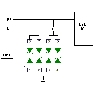
Protects two lines
Ultra Low Capacitance ,5pF
Cell phones
Audio/Video Inputs
Ethernet -10/100/1000 base T
Personal Digital Assistent (PDA)
USB Interface
SHORT PRODUCT APPLICATION NOTE
The SWPLCDA series of TVS arrays are designed to protect sensitive equipments which are connected to data and transmission lines from voltage surges caused by electrostatic discharge (ESD), electrical fast transients (EFT), and lightning.TVS diodes are characterized by their high surge capability, low operating and clamping voltages, and fast response time.The SWPLCDA series is designed to be used in parallel.
SEMICONDUCTOR-THIN FILM MANUFACTURING PROCESS DESCRIPTION
Integrated passive networks are manufactured using advanced thin film technologies including ultra -stable and self passivating Tantalum Nitride resistors, gold interconnect metallization and reliable MNOS capacitors to achieve excellent uniformity, performance and reliability. Thin film resistor technology is the preferred solution for all applications that require low noise, long term stability and excellent performance at very high frequencies. Semiconwell employs proprietary thin film technologies for deposition of a wide range of sheet resistance films from 1W/sq to 10,000 W/sq. All Semiconwell's products are available in die form and as KGD, known good die and are ideal for high reliability hybrid and multi chip module applications. Besides thin film resistors, Semiconwell integrates capacitors, Schottky diodes, Zener diodes and transistors. Integrated passive and active networks are manufactured using Semiconwell's in house high reliability semiconductor manufacturing processes. All semiconductor devices employ precision doping via ion implantation, silicon nitride junction passivation, platinum silicided contacts and gold interconnect metallization for best performance and reliability. MNOS capacitors and Tantalum Nitride resistors are easily integrated with Schottky diodes to provide complete standard and custom RCD solutions. In die form, these products are ideal for hybrid and multi chip module applications. In packaged form, these products are the best solution where space and weight are a concern.
ABSOLUTE MAXIMUM RATINGS
PARAMETER RATING UNITS
Operating Temperature Range -55 to +150 °C
Storage Temperature Range -55 to +150 °C
Peak Pulse Power (tp=8/20 µs) 500 W
Stresses beyond listed absolute maximum ratings may cause permanent damage to the device.
ELECTRICAL CHARACTERISTICS , TA=25 °C unless otherwise specified
PARAMETER VALUE UNITS
Reverse Stand-off Voltage 5 V
Diode Leakage Current, V=stand-off voltage max 20 µA
Breakdown Voltage ,I=1mA min. 6 V
Clamping Voltage,Ip=1A max.9.8V
Clamping Voltage,Ip=42A,8/20µs max.13.5 V
Capacitance, VIN=0V DC, f=1MHz max. 5 pF
GENERAL DIE INFORMATION
Substrate Thickness (mils) Die size (mils) Bonding pads Backside metal
SiO2 / Silicon 10±2 4X4 mils, 3µm thick 99.99% electroplated gold with TiW barrier that withstand 30 min at 400 °C in air without loss of adhesion. Au/Si compatible with eutectic and conductive epoxy die atach.
All Semiconwell products are available in die form for chip and wire hybrid circuits and multi chip modules applications. Typical delivery for standard die products is 3-4 weeks ARO. For Chip Scale Packaged (CSP) devices consult factory for an update on availability of certain products.
DIODES RESISTORS CAPACITORS
The diodes offer basic ESD protection, with low forward voltage, low leakage and low power dissipation in OFF state. Ultra stable TaN with low TCR <75ppm/°C typical. For Rsq<10W/sq and Rsq>500W/sq, resistive material is proprietary. Power rating/resistor max 100mW for R<1KW and 25mW for R>1KW. Standard tolerance is ±5%. Silicon nitride dielectric, MNOS capacitors exhibit high stability, low temperature coefficients, low leakage <10nA and high BV>50V.
DIE LAYOUT PACKAGE PIN OUT
STANDARD PRODUCTS ORDERING INFORMATION
SW PART # QUANTITY SOIC8 U/P($)
SWPLCDA05 5,000pc -SO8
SWPLCDA05 10,000pc -SO8
For products sold as bare tested die or known good die KGD, minimum order is 5000pc. Dice are 100% functional tested, visual inspected and shipped in antistatic waffle packs. For special die level KGD requirements, different packaging or custom configurations, contact sw_sales@semiconwell.com
Semiconwell P/N Quantity E-mail
Receive Instant Quote
Delivery for packaged RCD standard products is 6-8 weeks ARO. Certain items may be available from stock. For standard products available from stock, there is a minimum line item order of $250.0. Inventory is periodically updated. For 2500pc or larger orders, all surface mount packaged devices are shipped in tape on reel (T/R). For smaller quantities, it may vary. Samples are available only for customers that have issued firm orders pending qualification of product in a particular application. On line Orders have to be verified, accepted and acknowledged by Semiconwell sales department in writing before, becoming non cancelable binding contracts.
Semiconwell guarantees continuous supply and availability of any of it's standard products provided minimum order quantities are met.
SEMICONWELL has made every effort to have this information as accurate as possible. However, no responsibility is assumed by SEMICONWELL for its use, nor for any infringements of rights of third parties which may result from its use. SEMICONWELL reserves the right to revise the content or modify its product line without prior notice. SEMICONWELL products are not authorized for and should not be used within support systems which are intended for surgical implants into the body, to support or sustain life, in aircraft, space equipment, submarine, or nuclear facility applications without the specific written consent.
|