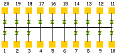
PAC DN027, PACDN027 same as SW TVS30KV, SWTVS30KV 30kV 17 CHANNEL Transient Voltage Suppressor TVS ARRAY manufactured by SEMICONWELL FEATURES APPLICATIONS 17 transient voltage suppressors in a single package ESD protection of PC parallel ports In-system ESD protection to 30kV contact discharge per IEC 61000-4-2 International Standard. Protection of interface ports or IC pins which are exposed to high levels of ESD discharge. Compact 20-pin QSOP package saves board space and eases layout in space critical applications SHORT PRODUCT APPLICATION NOTE Semiconwell' SWTVS -30KV is a transient voltage suppressor array that provides a very high level of protection for sensitive integrated circuit terminals that may be subjected to electrostatic discharge (ESD). The SWTVS-30KV is designed and characterized to safely dissipate ESD strikes al levels well beyond the maximum requirements set forth in the IEC61000-4-2 specification (Level4,8KV contact discharge). All pins of the SWTVS-30KV are rated at 30KV using the IEC6100-4-2 contact discharge method. SEMICONDUCTOR-THIN FILM MANUFACTURING PROCESS DESCRIPTION Integrated passive networks are manufactured using advanced thin film technologies including ultra -stable and self passivating Tantalum Nitride resistors, gold interconnect metallization and reliable MNOS capacitors to achieve excellent uniformity, performance and reliability. Thin film resistor technology is the preferred solution for all applications that require low noise, long term stability and excellent performance at very high frequencies. Semiconwell employs proprietary thin film technologies for deposition of a wide range of sheet resistance films from 1W/sq to 10,000 W/sq. All Semiconwell's products are available in die form and as KGD, known good die and are ideal for high reliability hybrid and multi chip module applications. Besides thin film resistors, Semiconwell integrates capacitors, Schottky diodes, Zener diodes and transistors. Integrated passive and active networks are manufactured using Semiconwell's in house high reliability semiconductor manufacturing processes. All semiconductor devices employ precision doping via ion implantation, silicon nitride junction passivation, platinum silicided contacts and gold interconnect metallization for best performance and reliability. MNOS capacitors and Tantalum Nitride resistors are easily integrated with Schottky diodes to provide complete standard and custom RCD solutions. In die form, these products are ideal for hybrid and multi chip module applications. In packaged form, these products are the best solution where space and weight are a concern. ESD Transient Voltage Suppressor Array SW TVS-30KV 17 transient voltage suppressors in a single package In-system ESD protection to 30kV contact discharge per IEC 61000-4-2 International Standard. Compact 20-pin QSOP package saves board space and eases layout in space critical applications ESD protection of PC parallel ports Protection of interface ports or IC pins which are exposed to high levels of ESD discharge. Semiconwell' SWTVS -30KV is a transient voltage suppressor array that provides a very high level of protection for sensitive integrated circuit terminals that may be subjected to electrostatic discharge (ESD). The SWTVS-30KV is designed and characterized to safely dissipate ESD strikes al levels well beyond the maximum requirements set forth in the IEC61000-4-2 specification (Level4,8KV contact discharge). All pins of the SWTVS-30KV are rated at 30KV using the IEC6100-4-2 contact discharge method. Integrated passive networks are manufactured using advanced thin film technologies including ultra-stable and self passivating Tantalum Nitride resistors, gold interconnect metallization and reliable MNOS capacitors to achieve excellent uniformity, performance and reliability. Thin film resistor technology is the preferred solution for all applications that require low noise, long term stability and excellent performance at very high frequencies. Semiconwell employs proprietary thin film technologies for deposition of a wide range of sheet resistance films from 1W/sq to 10,000 W/sq. All Semiconwell's products are available in die form and are ideal for high reliability hybrid and multi chip module applications.


SEMICONWELL
Integrated Passive Networks
  ESD Transient Voltage Suppressor Array
SW TVS-30KV


FEATURES
APPLICATIONS
SCHEMATIC
17 transient voltage suppressors in a single package
In-system ESD protection to 30kV contact discharge per IEC 61000-4-2 International Standard.
Compact 20-pin QSOP package saves board space and eases layout in space critical applications
Low supply and leakage currents
Small package
Lead-free versions available
ESD protection of PC parallel ports
Protection of interface ports or IC pins which are exposed to high levels of ESD discharge.
DVI ports
Expansion ports for Notebook/Handheld Computers
5V pseudo RS-232 ports
schematic

SHORT PRODUCT APPLICATION NOTE
Semiconwell' SWTVS -30KV is a transient voltage suppressor array that provides a very high level of protection for sensitive integrated circuit terminals that may be subjected to electrostatic discharge (ESD). The SWTVS-30KV is designed and characterized to safely dissipate ESD strikes al levels well beyond the maximum requirements set forth in the IEC61000-4-2 specification (Level4,8KV contact discharge). All pins of the SWTVS-30KV are rated at 30KV using the IEC6100-4-2 contact discharge method.

SEMICONDUCTOR-THIN FILM MANUFACTURING PROCESS DESCRIPTION
Integrated passive networks are manufactured using advanced thin film technologies including ultra -stable and self passivating Tantalum Nitride resistors, gold interconnect metallization and reliable MNOS capacitors to achieve excellent uniformity, performance and reliability. Thin film resistor technology is the preferred solution for all applications that require low noise, long term stability and excellent performance at very high frequencies. Semiconwell employs proprietary thin film technologies for deposition of a wide range of sheet resistance films from 1W/sq to 10,000 W/sq. All Semiconwell's products are available in die form and as KGD, known good die and are ideal for high reliability hybrid and multi chip module applications. Besides thin film resistors, Semiconwell integrates capacitors, Schottky diodes, Zener diodes and transistors. Integrated passive and active networks are manufactured using Semiconwell's in house high reliability semiconductor manufacturing processes. All semiconductor devices employ precision doping via ion implantation, silicon nitride junction passivation, platinum silicided contacts and gold interconnect metallization for best performance and reliability. MNOS capacitors and Tantalum Nitride resistors are easily integrated with Schottky diodes to provide complete standard and custom RCD solutions. In die form, these products are ideal for hybrid and multi chip module applications. In packaged form, these products are the best solution where space and weight are a concern.

ABSOLUTE MAXIMUM RATINGS
Reverse voltage VR Continuous IF IFRM for tw<100ms Max Power dissipation
7V 100mA 200 mA (20%duty cycle) 100mW@70°C/channel

Stresses beyond listed absolute maximum ratings may cause permanent damage to the device.

ELECTRICAL CHARACTERISTICS
PARAMETER VALUE UNITS
Reverse Stand-off Voltage,I=10µA
min 5.5
V
Signal Clamp Voltage , Positive Clamp, 20 mA
min 5.6:typ.6.8 ;max. 8.0
V
Signal Clamp Voltage , Negative Clamp, 20 mA
min -1.2:typ.-0.8 ;max. -0.4
V

In-system ESD withstand voltage (note 1)
Human Body Model (MIL-STD-883D,method 3015)
IEC61000-4-2, contact discharge method


min ±30
min ±30


KV
KV

Clamping voltage during ESD discharge, Positive
MIL-STD-883D (Method 3015) ,8KV , Negative

typ.9.5
typ.-0.4

V
V

Capacitance @ 2.5V dc, 1 MHz
typ.175
pF
Operating Temperature
-20 to +85
°C
Storage Temperature
-65 to +150
°C
Package Power Rating
max.1.0
W
Note 1: ESD applied between channel pin and ground, one at a time. All other pins are open. Pins 4,5,6 grounded. This parameter is guaranteed by design and characterization.

GENERAL DIE INFORMATION
Substrate Thickness (mils) Die size (mils) Bonding pads Backside metal
SiO2 / Silicon 10±2 90 x 60 ±3 4X4 mils, 3µm thick 99.99% electroplated gold with TiW barrier that withstand 30 min at 400 °C in air without loss of adhesion. Au/Si compatible with eutectic and conductive epoxy die atach.
All Semiconwell products are available in die form for chip and wire hybrid circuits and multi chip modules applications. Typical delivery for standard die products is 3-4 weeks ARO. For Chip Scale Packaged (CSP) devices consult factory for an update on availability of certain products.

DIODES CONDUCTORS CAPACITORS
TVS diodes using solid state silicon avalanche technology are characterized by their high surge capability, low operating and clamping voltages, fast response time and low leakage current The bonding pads are gold with a TiW barrier that withstands 30 min at 400°C in air without loss of adhesion. Silicon nitride dielectric, MNOS capacitors exhibit high stability, low temperature coefficients, low leakage <10nA and high BV>50V.

DIE LAYOUT PACKAGE PIN OUT
layout / design pending schematic
Vch=1,2,3,7,8,9,10,11,12,13,14,15,16,17,18,19,20
Vss=4,5,6

STANDARD PRODUCTS ORDERING INFORMATION

SW PART # QUANTITY SOIC-20 U/P($) QSOP-20 U/P($) TQSOP-20 U/P($) TSSOP-20 U/P($) PDIP-20 U/P($) BARE DIE U/P($)
SWTVS-30kV17 5000pc -20SO   -20QS   -20TQS   -20TS   -20DP   -20BD  
SWTVS-30kV17 10,000pc -20SO   -20QS   -20TQS   -20TS   -20DP   -20BD  
For products sold as bare tested die or known good die KGD, minimum order is 5000pc. Dice are 100% functional tested, visual inspected and shipped in antistatic waffle packs. For special die level KGD requirements, different packaging or custom configurations, contact sw_sales@semiconwell.com

  Semiconwell P/N Quantity E-mail    
Receive Instant Quote
 

Delivery for packaged RCD standard products is 6-8 weeks ARO. Certain items may be available from stock. For standard products available from stock, there is a minimum line item order of $250.0. Inventory is periodically updated. For 2500pc or larger orders, all surface mount packaged devices are shipped in tape on reel (T/R). For smaller quantities, it may vary. Samples are available only for customers that have issued firm orders pending qualification of product in a particular application. On line Orders have to be verified, accepted and acknowledged by Semiconwell sales department in writing before, becoming non cancelable binding contracts.

Semiconwell guarantees continuous supply and availability of any of it's standard products provided minimum order quantities are met.

SEMICONWELL has made every effort to have this information as accurate as possible. However, no responsibility is assumed by SEMICONWELL for its use, nor for any infringements of rights of third parties which may result from its use. SEMICONWELL reserves the right to revise the content or modify its product line without prior notice. SEMICONWELL products are not authorized for and should not be used within support systems which are intended for surgical implants into the body, to support or sustain life, in aircraft, space equipment, submarine, or nuclear facility applications without the specific written consent.

Home Product Tree Tech. Support Print PDF Packages Request Quote Inventory Place Order Contact sales